T507 / T517
The H616 die in a larger 15 x 15 mm TFBGA421 that brings out what the TV-box package hides: dual-link LVDS and RGB panels, a 4-lane MIPI CSI and a parallel camera port, two Ethernet MACs to external PHYs, rated -40 to 85 C; no PCIe, no USB 3.0, no NPU, and HDMI only on one ordering code. Bare chip USD 8.47 to 13.08 on LCSC.
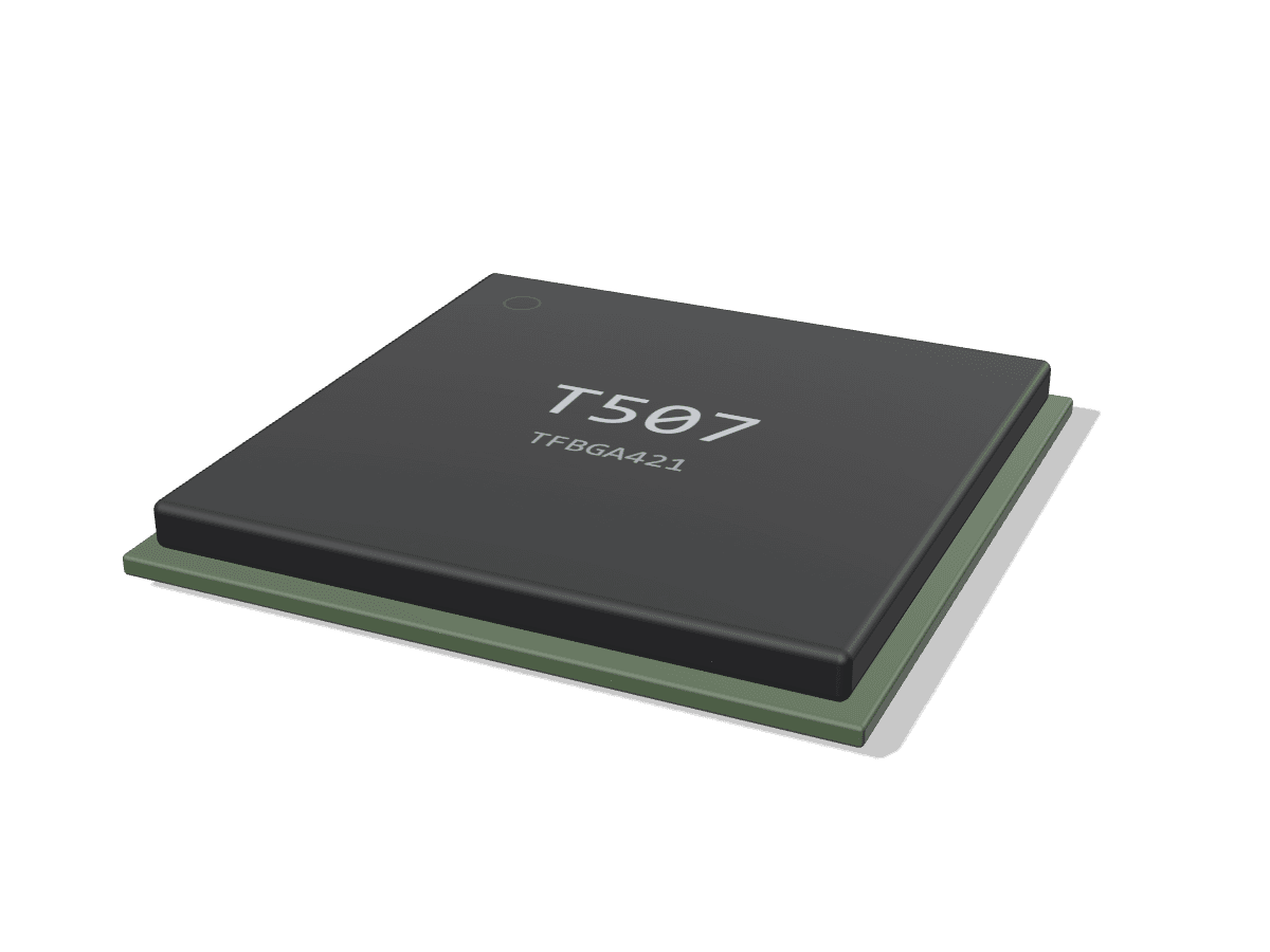
- CPU
- 4x A53 up to 1.5 GHz
- GPU
- Mali-G31 MP2
- NPU
- None
- Video
- 4K60 H.265/VP9 dec, 4K25 H.264 enc
- PCIe
- None
What the T507 / T517 is for
Right for
- Surround-view (AVM) and DVR boxes: one 4-lane MIPI CSI at up to 1 Gbps per lane (8 MP at 30 fps or 4x 1080p25) plus a parallel port taking BT.656 at up to 4x 720p30, with a 4K25 H.264 encoder
- Industrial and in-vehicle HMI on LVDS or RGB panels: dual-link LVDS up to 1920 x 1080 at 60 fps, single link to 1366 x 768, or RGB888 to 1080p60, with CVBS out as a second display
- Products that need a -40 to 85 C ambient rating on a cheap, well understood quad A53: the same die as the H616/H618, so the community kernel, U-Boot and TF-A work for the H616 applies
- Two-port Ethernet gateways and terminals: EMAC0 gigabit (RGMII or RMII) and EMAC1 10/100 (RMII), both to external PHYs and usable at once
- Media playback panels: H.265 Main10, VP9 and AVS2 decode to 4K60 and H.264 to 4K30
Wrong for
- Anything needing PCIe, USB 3.0 or SATA: the datasheet lists one USB 2.0 OTG and three USB 2.0 hosts and nothing faster
- HDMI on the plain T507 or the T517: datasheet Rev 1.3 restricts HDMI to the T507 CX00H0YZ ordering code
- MIPI DSI or eDP panels: outputs are RGB, LVDS, serial RGB, i8080, BT.656, CVBS and (CX00H0YZ only) HDMI
- On-device AI or more than 4 GB of DRAM: there is no NPU and the DRAM controller is 32-bit to 4 GB
- Products that must run display or camera on mainline Linux today: no H616-family TCON, LVDS, HDMI or CSI driver is in any release as of v7.3-rc7
Cost and constraints
- BOM floor is the SoC (USD 8.47 at 126 to USD 13.08 at 1 on LCSC), an X-Powers PMIC (AXP853T on the MYIR MYC-YT507H), 32-bit DDR3/DDR3L/DDR4/LPDDR3/LPDDR4, a 24 MHz crystal and external Ethernet PHYs
- TFBGA421, 15 x 15 mm, 0.65 mm ball pitch, 0.35 mm balls; public modules are 10-layer (MYIR MYC-YT507H)
- DRAM is capped at 792 MHz for every type in the datasheet, so LPDDR4 runs well below its rated speed
- Pick the ordering code before layout: HDMI exists only on T507 CX00H0YZ, and the T517 uses gold bond wires where the T507 uses copper
- Production software is the Allwinner 4.9.170 BSP (Android 10, Buildroot, Ubuntu 18.04 rootfs) as shipped by module vendors; no newer public BSP kernel was found
Inside the T507 / T517
Drawn by Groundplane from the datasheet rev 1.3. Not Allwinner artwork.
- 32-bit DDR3/DDR4/LPDDR3/4
- eMMC 5.0 (8-bit)
- SD 3.0 / SDIO 3.0
- SPI NOR or SPI NAND
- 8-bit raw NAND
- 4x Cortex-A53 up to 1.5 GHz
- 512 KB L2, NEON, TrustZone
- Mali-G31 MP2
- G2D 2D engine, 2048x2048
- De-interlacer with TNR
- H.265/VP9/AVS2 4K60 decoder
- H.264 4K30 decoder
- H.264 4K25 encoder
- JPEG codec
- 32-bit DRAM controller
- DDR3/DDR4/LPDDR3/LPDDR4
- IOMMU for DE, VE, CSI, G2D
- Display engine to 4096x2048
- TCON LCD: RGB, dual LVDS
- TV encoder (CVBS)
- HDMI TX (CX00H0YZ only)
- MIPI CSI-2, 4 lanes
- Parallel CSI, BT.656/1120
- Secure boot ROM
- Crypto engine, TRNG
- 2 Kbit eFuse (SID)
- CCU, 13 PLLs, 24 MHz DCXO
- 16-ch DMA, timers, RTC
- 4 thermal sensors
- Audio hub, DAC, DMIC
- USB 2.0 OTG (FEL port)
- 3x USB 2.0 host
- GbE MAC (RGMII/RMII)
- 10/100 MAC (RMII)
- Dual LVDS or RGB, CVBS
- MIPI CSI x4, parallel CSI
- I2S/TDM x3, PDM, S/PDIF
- UART x6, TWI x6, SPI x2
- PWM x6, GPADC x4, TSC, SCR
Read from the documents
Each value names the document it was read from.
| CPU | 4x Cortex-A53, ARMv8, 32 KB L1 I and D per core, 512 KB L2, NEON, VFPv4, TrustZone, LPAE | Datasheet Rev 1.3, 2.1 |
|---|---|---|
| CPU clock | Up to 1.5 GHz in the 2019 T5 Series brief and on Allwinner's T517 page; Allwinner's current T507 page says up to 1.4 GHz. The datasheet states no clock | Product brief, Specifications |
| GPU | Mali-G31 MP2; OpenGL ES 1.0/2.0/3.2, Vulkan 1.1, OpenCL 2.0 | Datasheet Rev 1.3, 2.2 |
| NPU | None | Datasheet Rev 1.3, 2 |
| Video decode | H.265 Main10 L5.1, VP9 Profile 2 and AVS2 10-bit up to 4K60; H.264 BP/MP/HP L4.2 up to 4K30; H.263, MPEG-1/2/4, Xvid, Sorenson Spark, VP8, AVS/AVS+, VC-1 up to 1080p60 | Datasheet Rev 1.3, 2.4.1 |
| Video encode | H.264 BP/MP/HP up to 4K25 (4096 x 4096 max), I/P frames, single reference, CBR/VBR 256 kbit/s to 100 Mbit/s, 8 ROIs | Datasheet Rev 1.3, 2.4.2 |
| JPEG | JPEG decode up to 45 MPPS; MJPEG/JPEG baseline encode, 1080p60 snapshot | Datasheet Rev 1.3, 2.4.1, 2.4.2 |
| Memory | 32-bit DDR3, DDR3L, DDR4, LPDDR3 or LPDDR4, up to 4 GB, at most 792 MHz for every type | Datasheet Rev 1.3, 2.3.2 |
| Storage | eMMC 5.0 (8-bit, HS-DDR 100 MHz at 1.8 V), SD 3.0, SDIO 3.0, 8-bit raw NAND (ONFI 2.0, Toggle 2.0, SLC/MLC/TLC, 80-bit ECC per 1 KB), SPI NOR and SPI NAND boot | Datasheet Rev 1.3, 2.3.1 to 2.3.4 |
| Display | RGB DE/SYNC to 1920 x 1080 at 60 fps; dual-link LVDS to 1920 x 1080 at 60 fps, single link to 1366 x 768 (LVDS shares the RGB pins); serial RGB and i8080 to 800 x 480; BT.656 out; CVBS (PAL/NTSC); HDMI 2.0 to 4K60 with HDCP 2.2, CEC and HDR10 only on T507 CX00H0YZ. Display engine to 4096 x 2048 with write-back for dual display | Datasheet Rev 1.3, 1.1, 2.5.1, 2.8 |
| Camera | One 4-lane MIPI CSI-2 (v1.0, up to 1.0 Gbps per lane, 8 MP at 30 fps or 4x 1080p25) and one parallel port (8-bit DC, BT.656, BT.601, BT.1120, up to 4x 720p30 time-multiplexed, 148.5 MHz pixel clock); no ISP is listed | Datasheet Rev 1.3, 2.7 |
| PCIe | None | Datasheet Rev 1.3, 2.11 |
| SATA | None | Datasheet Rev 1.3, 2.11 |
| USB | 1x USB 2.0 OTG (USB0, also the FEL port), 3x USB 2.0 host, all with integrated PHYs | Datasheet Rev 1.3, 2.11.1 |
| Ethernet | EMAC0 10/100/1000 with RGMII or RMII; EMAC1 10/100 with RMII; both to external PHYs and usable at once. No embedded PHY (unlike the H616 package) | Datasheet Rev 1.3, 2.11.2 |
| Audio | Stereo DAC (differential or single-ended line out, 95 dB SNR), audio hub with 3 external I2S/PCM/TDM (up to 16 ch), up to 8 PDM microphones, S/PDIF (OWA) out. No analog ADC input | Datasheet Rev 1.3, 2.9 |
| Security | Crypto engine (AES, DES, 3DES, XTS, MD5, SHA-1 to SHA-512, HMAC, RSA to 4096, ECC to 521), 160-bit PRNG, 256-bit TRNG, 2 Kbit eFuse with secure zone, secure boot (X.509), secure memory and peripheral control | Datasheet Rev 1.3, 2.10 |
| Other I/O | 6x UART (two 2-wire, four 4-wire), 2x SPI (quad), 6x TWI, 6-ch PWM, 4-ch 12-bit GPADC, 1-ch LRADC, CIR receiver, transport stream controller with DVB-CSA, smart card reader | Datasheet Rev 1.3, 2.11.3 to 2.11.11 |
| Process | 28 nm HPC | Product brief, Process |
| Package | TFBGA421, 15 x 15 mm, 0.65 mm ball pitch, 0.35 mm balls; MSL3; 126 per tray | Datasheet Rev 1.3, 2.12, 8.1, 8.2 |
| Temperature | Ambient -40 to 85 C; junction -40 to 120 C recommended, 125 C absolute maximum. The T5 series is qualified to AEC-Q100 | Datasheet Rev 1.3, 1, Table 5-1, Table 5-2 |
| Thermal | theta-JA 26, theta-JB 10.34, theta-JC 10.14 C/W (JEDEC JESD51); four sensors in GPU, VE, CPU and DDR | Datasheet Rev 1.3, Table 6-1, 2.6.7 |
Variants
| T507 | Copper bond wire, no HDMI (datasheet Rev 1.3 Table 1-1). Allwinner's current page lists the CPU at up to 1.4 GHz and decode at 4K30. Same die as H616: TF-A and the Linux pinctrl commit say so. | Datasheet Rev 1.3 |
|---|---|---|
| T507 CX00H0YZ | Copper bond wire, adds the HDMI 2.0 TX (4K60, HDCP 2.2) and its VCC_HDMI rail. Added in datasheet Rev 1.3. | Datasheet Rev 1.3 |
| T507-H | The name MYIR uses on its MYC-YT507H module, which it lists at 1.5 GHz with an HDMI 2.0a output. No Allwinner document names a T507-H; whether it is the CX00H0YZ code is not confirmed. | Other |
| T517 | Gold bond wire, no HDMI. Allwinner's T517 page states AEC-Q100 and 1.5 GHz, and lists 6 SPI where the T507 page lists 2. | Datasheet Rev 1.3 |
| H616 / H618 (sibling) | Same die in a TFBGA284 14 x 12 mm package with an internal 100M PHY on EMAC1 and no LCD or camera pins, rated -20 to 70 C. Covered on the H618 page. | Other |
What to watch when you design with it
Power and PMIC
Datasheet rails: VDD_CPU 0.81 to 1.1 V, VDD_GPU and VDD_SYS 0.81 to 0.99 V, 1.8 V for AVCC, PLL, DCXO, RTC, LVDS, MIPI CSI, TV out and VDD18_DRAM, 3.3 V for VCC_IO, VCC_PA, VCC_PI and USB; VCC_PC, VCC_PD, VCC_PE and VCC_PG are selectable (1.8 or 3.3 V, plus 2.5 V on PD and 2.8 V on PE for camera sensors). The power-on table orders VCC_RTC, then VDD_SYS, then VDD_CPU with AVCC/PLL/DCXO, VDD18_DRAM and (DDR4) VPP_DRAM, then VCC_DRAM and the I/O rails, then RESET; each step starts once the previous rail is within 90 to 110 percent. Power-off has no restriction. MYIR fits an X-Powers AXP853T on its MYC-YT507H; linux-sunxi lists the AXP853T as a variant of the AXP15060, which mainline Linux supports since 6.5. Allwinner publishes no power consumption figures; the datasheet says to ask its FAE.
Sources: Datasheet Rev 1.3, Other, linux-sunxi.org
DDR
One 32-bit channel to 4 GB, DDR3, DDR3L, DDR4, LPDDR3 or LPDDR4, each capped at 792 MHz. VCC_DRAM is 1.1 V for LPDDR4, 1.2 V for DDR4 and LPDDR3, 1.35 V for DDR3L and 1.5 V for DDR3; VDD18_DRAM is 1.8 V and DDR4 also needs a 2.5 V VPP that ramps before VCC_DRAM. Public modules use DDR3L (Forlinx FETT507-C) and LPDDR4 (MYIR MYC-YT507H). Mainline U-Boot's open-source H616 DRAM driver supports DDR3, LPDDR3 and LPDDR4 but not DDR4. Allwinner's DRAM layout rules are not public.
Sources: Datasheet Rev 1.3, Other, Other, github.com
High-speed interfaces
There is no SerDes, so the fast links are DRAM, the MIPI CSI (4 data lanes plus clock at up to 1 Gbps per lane), LVDS, RGMII and four USB 2.0 ports. LVDS shares the PD-bank pins with the RGB and transport stream functions and has its own 1.8 V VCC_LVDS, so a design gets LVDS or RGB, not both. Unlike the H616 package there is no internal 100M PHY: EMAC1 is an RMII on the PA bank (PA0 to PA9 with MDC and MDIO) for an external PHY, and EMAC0 supports RGMII or RMII. Forlinx OKT507-C brings out one gigabit and one fast Ethernet port this way.
Sources: Datasheet Rev 1.3, Other, github.com
Boot and FEL
The BROM reads the FEL pin (ball D10): high runs the media boot, low enters the USB mandatory-upgrade mode on USB0 OTG. Boot media are chosen either by GPIO straps or by eFuse (BOOT_MODE bit in the SID). In GPIO mode five strap bits, BOOT_SEL and BOOT_SEL[4:1] (shared with PC3 to PC6, the NAND and SPI0 and SMHC2 pins), pick the order, and every listed order starts with SMHC0 (the SD card): SD then SPI NAND, SD then SPI NOR, SD then eMMC boot then user area, and SD then SLC or MLC NAND. The eFuse try order is SMHC0, SMHC2, NAND, SPI NOR, SPI NAND. sunxi-fel handles the die as SoC ID 0x1823 (H616) from git master. Keep the OTG port and a FEL button or test pad on every board.
Sources: Datasheet Rev 1.3, TRM Rev 1.3, github.com
Thermal
theta-JA is 26 C/W, theta-JB 10.34 C/W and theta-JC 10.14 C/W per JEDEC JESD51, with a recommended junction maximum of 120 C at up to 85 C ambient. The four on-chip sensors (GPU, VE, CPU, DDR) are the same as the H616, and mainline has the thermal driver since 6.9 and cpufreq since 6.10 for that die. Forlinx and MYIR rate their modules -40 to 85 C.
Sources: Datasheet Rev 1.3, Other, Other
Gotchas
HDMI is not on the plain T507 after datasheet Rev 1.3: order the CX00H0YZ code if you need it, and check the marking on samples. Allwinner's own pages now quote 1.4 GHz and 4K30 decode for the T507, below the datasheet and brief, so do not design a product around 4K60 decode or 1.5 GHz without confirming with Allwinner or your module vendor. On Allwinner GPIO, a write to a bank can corrupt the output latch of pins muxed as inputs; a fix found on a T507 board bit-banging I2C on port E landed in Linux 7.3-rc5, so vendor 4.9 kernels still carry the bug for emulated open-drain lines. Mainline describes the full T507 pinout (banks A, D and E added in 6.7) and the LCD TCON clocks and LVDS reset (6.15, 6.16), but no TCON, LVDS, HDMI or CSI driver yet.
Sources: Datasheet Rev 1.3, Other, github.com, github.com
Layout guides for the T507 / T517's interfaces
Public layout guidance for each interface this chip has, from vendors who publish it, plus our calculators.
LPDDR4
Point-to-point routing; TI notes that on-die termination on both ends means no board termination is needed. Byte lanes length-matched to their strobe and command/address matched to the clock, all over a solid reference plane. Impedance targets differ by vendor: TI AM62x and ADI EE-480 use 40 ohm single-ended and 80 ohm differential, Synaptics SL1680 uses 50 and 85 ohm, AMD Versal 45 and 82 ohm. Use the SoC vendor's own target and simulate.
- AM62x, AM62Lx DDR Board Design and Layout GuidelinesTexas Instruments, SPRAD06, C, 2025
- AM62Ax, AM62Px, AM62Dx LPDDR4 Board Design and Layout GuidelinesTexas Instruments, SPRAD66, B, 2024
- ADSP-2184x/ADSP-SC84x LPDDR4 Board Design GuidelinesAnalog Devices, EE-480, 1, 2026
- SL1680 General PCB Design and LPDDR4 & LPDDR4(x) Interface Layout GuidelinesSynaptics, PN 506-001390-01, E
- DDR length matching calculatorGroundplane calculator
DDR4
DDR4 uses pseudo open-drain data signaling and needs a VPP supply, with command/address routed fly-by or as a balanced tree depending on device count. TI AM62x uses 40 ohm single-ended and 80 ohm differential; AMD Versal uses 50 and 90 ohm, relaxed under the BGA. Match data to strobe per byte and command/address to clock.
- AM62x, AM62Lx DDR Board Design and Layout GuidelinesTexas Instruments, SPRAD06, C, 2025
- Versal Adaptive SoC PCB Design User Guide: PCB Routing Guidelines for DDR4 InterfacesAMD, UG863, 1.12, 2026
- SL1640 General PCB Design and DDR4 & LPDDR4(x) Interface Layout GuidelinesSynaptics, PN 506-001529-01, D
- PCB Design Guidelines (HSSI, EMIF, MIPI, True Differential, PDN) User Guide: Agilex 5 FPGAs and SoCsAltera, 821801, 2026
- DDR length matching calculatorGroundplane calculator
- Via current calculatorGroundplane calculator
DDR3 / DDR3L
Fly-by command/address with termination at the end of the chain, point-to-point data lanes matched to their strobe, and a clean VREF. ST recommends 55 ohm single-ended and 100 ohm differential for DDR3 and DDR3L on STM32MP1 boards, and shows that a 4-layer board is possible with strict layer allocation.
- STM32MP1 Series DDR memory routing guidelinesSTMicroelectronics, AN5122, 3, 2019
- DDR3 Design Requirements for KeyStone DevicesTexas Instruments, SPRABI1, D, 2022
- SL2610 General PCB Design and DDR3L/DDR4 & LPDDR4(x) Interface Layout GuidelinesSynaptics, PN 506-001629-01, A, 2025
- DDR length matching calculatorGroundplane calculator
LPDDR3
Point-to-point and normally unterminated, with command/address matched to the clock and each byte matched to its strobe. ST gives the same targets for LPDDR3 as for DDR3: 55 ohm single-ended and 100 ohm differential. Few current public guides cover LPDDR3, so treat the SoC vendor's reference layout as the stronger source.
- STM32MP1 Series DDR memory routing guidelinesSTMicroelectronics, AN5122, 3, 2019
- DDR length matching calculatorGroundplane calculator
eMMC
A single-ended bus: CLK, CMD, DAT0 to DAT7 and, for HS400, the data strobe. TI and Synaptics both route it at 50 ohm single-ended, match the group, and keep stubs short; Synaptics places a 22 or 33 ohm series resistor on CLK and STRB. At HS400 TI also checks the eMMC I/O supply impedance, not just the traces.
- AM62Px eMMC HS400 Board Design and Simulation GuidelinesTexas Instruments, SPRADP5, A, 2026
- Astra Machina Foundation Series eMMC ConfigurationSynaptics, PN 506-001594-01, D
- i.MX28 Layout and Design GuidelinesNXP (Freescale), AN4215, 0, 2010
SD card / SDIO
Single-ended CLK, CMD and four data lines over a solid ground plane, at constant trace width and matched length. NXP asks for clock-to-neighbor spacing greater than twice the trace height above the plane and 1.5 times for data and CMD, with 45 degree bends. UHS modes switch the I/O to 1.8 V, so a level translator often sits next to the socket.
- NVT4557/NVT4558/NVT4858 voltage-level translator layout guidelineNXP, AN13158, 1.1, 2022
- i.MX28 Layout and Design GuidelinesNXP (Freescale), AN4215, 0, 2010
- SD Physical Layer Simplified SpecificationSD Association, 9.10, 2023
PCIe
AC-coupled differential lanes routed with no stubs, minimal vias and back-drilled or blind vias where speed demands, with lane-to-lane skew handled by the receiver. Targets differ by guide: TI Jacinto 7 uses 85 ohm differential for lanes and 100 ohm for the reference clock, while TI's earlier SoC guide tabulates 100 ohm and, for some devices, 95 ohm. Match the target to your connector and stackup.
- Jacinto7 AM6x, TDA4x, and DRA8x High-Speed Interface Design GuidelinesTexas Instruments, SPRACP4, A, 2024
- High-Speed Interface Layout GuidelinesTexas Instruments, SPRAAR7, J, 2023
USB 2.0
One D+/D- pair at 90 ohm differential, routed in parallel for its whole length with minimal deviations at the connector and package. NXP keeps clocks and periodic signals at least 50 mils away and other signals at least 20 mils away from the pair.
- High-Speed Layout Guidelines for Signal Conditioners and USB HubsTexas Instruments, SLLA414, A, 2026
- High-Speed Interface Layout GuidelinesTexas Instruments, SPRAAR7, J, 2023
- i.MX28 Layout and Design GuidelinesNXP (Freescale), AN4215, 0, 2010
HDMI
Four TMDS pairs (three data, one clock) at 100 ohm differential, as both TI guides state, with tight intra-pair matching and as few vias as possible between the SoC and the connector. HDMI also needs 5 V supply switching, DDC and CEC level handling, hot-plug detect and ESD at the connector.
- High-Speed Layout Guidelines for Signal Conditioners and USB HubsTexas Instruments, SLLA414, A, 2026
- High-Speed Interface Layout GuidelinesTexas Instruments, SPRAAR7, J, 2023
- TPD12S016 PCB Layout Guidelines for HDMI ESDTexas Instruments, SLLA324, 2012
MIPI CSI-2
Same D-PHY rules as DSI: 100 ohm differential lanes in both TI guides, with lane-to-lane skew bounded (40 ps in TI Jacinto 7). Size the lane count and lane rate from the sensor's output format before routing.
- Jacinto7 AM6x, TDA4x, and DRA8x High-Speed Interface Design GuidelinesTexas Instruments, SPRACP4, A, 2024
- High-Speed Interface Layout GuidelinesTexas Instruments, SPRAAR7, J, 2023
- PCB Design Guidelines (HSSI, EMIF, MIPI, True Differential, PDN) User Guide: Agilex 5 FPGAs and SoCsAltera, 821801, 2026
- MIPI CSI-2 bandwidth calculatorGroundplane calculator
LVDS
Tightly coupled differential pairs terminated at the receiver in 100 ohm, with TI's EMI guide asking for 100 ohm differential traces within 5 percent. Keep pairs matched and away from other aggressors, and avoid stubs and reference plane gaps along the route to the panel connector.
- LVDS Owner's Manual: Including High-Speed CML and Signal ConditioningTexas Instruments, SNLA187, 4th edition, 2008
- High-Speed Layout Guidelines for Reducing EMI for LVDS SerDes DesignsTexas Instruments, SNLA302, 2018
- LVDS SerDes Gen I PCB and Interconnect Design-In GuidelinesTexas Instruments, SNLA008, A, 2018
Ethernet (RGMII / RMII)
TI routes MAC-to-PHY (MII family) traces at 50 ohm single-ended, under 6 inches, matched within 20 mils for gigabit, and the PHY-side MDI pairs at 100 ohm differential. RGMII also needs a 1.5 to 2.0 ns clock-to-data delay, added on the board or inside the MAC or PHY (RGMII-ID); decide which before layout so it is not applied twice.
- Ethernet PHY PCB Design Layout ChecklistTexas Instruments, SNLA387, 2021
- PCB Design Guideline for RGMII InterfaceRenesas, R01AN6272EJ0141, 1.41, 2026
- i.MX28 Layout and Design GuidelinesNXP (Freescale), AN4215, 0, 2010
SATA
AC-coupled TX and RX pairs at 100 ohm differential in TI's SoC guide, routed with the same via, stub and reference plane rules as PCIe and USB 3. On Rockchip parts SATA usually shares a combo PHY with PCIe or USB 3, so the lane is routed once to whichever connector the design picks.
- High-Speed Interface Layout GuidelinesTexas Instruments, SPRAAR7, J, 2023
- High-Speed Layout Guidelines for Signal Conditioners and USB HubsTexas Instruments, SLLA414, A, 2026
Board-level design guides
Impedance and timing, power, thermal and ESD guidance that applies to any board around this chip.
Impedance and timing
Every high-speed interface on the board comes down to the same two numbers: the trace impedance your stackup actually gives, and the delay each trace adds. Set the stackup with your fab first, then route to its impedance table and match lengths in time, not millimeters, where the layers differ.
- High-Speed Interface Layout GuidelinesTexas Instruments, SPRAAR7, J, 2023
- PCB impedance calculatorGroundplane calculator
- PCB propagation delay calculatorGroundplane calculator
Power delivery
For each switching regulator, place and route the input capacitor first, keep the switching current loop small, and keep the switch node short. Give the SoC rails solid planes and decoupling at the balls, and size current-carrying copper and vias for the real load.
- Five steps to a great PCB layout for a step-down converterTexas Instruments, SLYT614, 2015
- AN-1149 Layout Guidelines for Switching Power SuppliesTexas Instruments, SNVA021, C, 2013
- AN-1229 SIMPLE SWITCHER PCB Layout GuidelinesTexas Instruments, SNVA054, C, 2013
- Buck converter calculatorGroundplane calculator
- LDO power dissipation calculatorGroundplane calculator
- PCB trace width calculatorGroundplane calculator
- Via current calculatorGroundplane calculator
Thermal
Theta-JA is measured on a JEDEC test board that carries most of the heat, so it does not transfer directly to a product board; use it to compare packages and use the psi metrics for estimates. Thermal vias under the package, copper area and copper thickness move the most heat into the board.
- Semiconductor and IC Package Thermal MetricsTexas Instruments, SPRA953, D, 2024
- AN-2020 Thermal Design By Insight, Not HindsightTexas Instruments, SNVA419, C, 2013
- Heatsink thermal resistance calculatorGroundplane calculator
- LDO power dissipation calculatorGroundplane calculator
ESD protection
Place the TVS as close to the connector as design rules allow, route from the connector to the TVS with no stub, and keep the protected IC further from the TVS than the TVS is from the connector. Choose parts by clamping performance and by capacitance low enough for the interface speed.
- ESD Protection Layout GuideTexas Instruments, SLVA680, A, 2022
- Reading and Understanding an ESD Protection Data SheetTexas Instruments, SLLA305, A
- TPD12S016 PCB Layout Guidelines for HDMI ESDTexas Instruments, SLLA324, 2012
- PCB conductor spacing calculator (IPC-2221)Groundplane calculator
Allwinner's hardware design guide
Allwinner's hardware design guide, EVB reference schematics and DDR templates come from Allwinner or an authorized agent, usually under NDA, or through your SoM vendor. We do not link copies circulating elsewhere. The vendor schematics and open designs on the Boards tab are real, shipped layouts on the T507 / T517 and the best public reference.
BSP, mainline and toolkits
| Area | Status | Links |
|---|---|---|
| Vendor BSP kernel | Allwinner's sun50iw9 BSP, Linux 4.9.170 with U-Boot 2018.05 (brandy), as published by MYIR for the MYD-YT507H (myir-t5-kernel, branches develop and develop-android10, last push 2023-02). Forlinx ships Linux 4.9 with Qt 5.12, Android 10 and ForlinxDesktop 18.04 for the OKT507-C. No newer public T507 BSP kernel was found.Checked 2026-10-13 | |
| Mainline Linux | No T507 board device tree in torvalds/linux as of v7.3-rc7; a T507 board uses sun50i-h616.dtsi. T507-specific work that landed: GPADC driver naming the T507 (6.6), extra pinctrl muxes for banks A, D and E that only the T507 package exposes (6.7), LCD TCON clock and reset (6.15) and LVDS reset (6.16), and a pinctrl output-latch fix found on a T507 board (7.3-rc5). Everything the H616 has applies (CPU, MMC, USB, EMAC0, thermal, cpufreq, crypto, Panfrost GPU 6.16). Not in any release: TCON, LVDS and HDMI output, CSI capture, EMAC1, PWM and the cedrus video decoder.Checked 2026-10-13 | |
| U-Boot | Mainline U-Boot covers the die through MACH_SUN50I_H616, with the open-source DRAM driver (DDR3, LPDDR3, LPDDR4; no DDR4) and die revision 2 handling since v2023.07. v2026.10 has no T507 board defconfig, so a T507 board starts from an H616 one.Checked 2026-10-13 | |
| TF-A and SCP | TF-A platform sun50i_h616 lists H313, H616, H700 and T507. T507 support, including the second die revision with per-core CPU control registers, merged 2023-05-04 and shipped in v2.9. No ARISC management core, so crust/SCP firmware does not apply.Checked 2026-10-13 | |
| FEL tools | sunxi-fel recognizes the die as SoC ID 0x1823 (H616) in git master; the last tagged release is from 2016. Vendors flash with Allwinner PhoenixSuit; jejezz/allwinner-flashing-tool-macos is an open-source FEL/EFEX flasher that names T507 and T527 boards.Checked 2026-10-13 | |
| Android | Android 10 on the vendor BSP: MYIR publishes its MYD-YT507H Android 10 manifest and device trees; Forlinx ships Android 10 for the OKT507-C.Checked 2026-10-13 | |
| Distributions | Vendor images only: MYIR Buildroot with Qt 5.12.5, Ubuntu 18.04 and Android 10; Forlinx Linux with Qt 5.12, ForlinxDesktop 18.04 and Android 10. No T507 board in Armbian, OpenWrt or Buildroot upstream.Checked 2026-10-13 | |
| Community | linux-sunxi has a T507 page and hosts the T5 series datasheet, user manual and the MYD-YT507H board files on its download server; the H616 page and mailing list carry the shared mainline work.Checked 2026-10-13 |
T507 / T517 system on modules
Any of these can sit on a carrier board we design.
| Module | Vendor | Connector | RAM | Design files | Price |
|---|---|---|---|---|---|
| FETT507-C | Forlinx | 3x 80-pin board-to-board, 0.5 mm pitch (240 pins) | 1 or 2 GB DDR3L | Brief PDF and online hardware manual public; datasheet, carrier schematic and PCB, pinmux after purchase | |
| MYC-YT507H | MYIR | 164-pin castellated edge plus 58-pin LGA, 1.0 mm pitch | 1 or 2 GB LPDDR4 (3 or 4 GB optional) | Product PDF, STEP model and CE certificate public; carrier schematics and design guide on request | USD 66 (MYIR sample price, 1 GB) |
| MINI507 | Boardcon | 2x 100-pin Hirose DF40, 0.4 mm pitch (carrier side DF40C-100DS-0.4V) | 2 or 4 GB DDR4 | Reference user manual (pinout, power tree, peripheral reference circuits) and 3D model public | |
| SOM-TLT507 | Tronlong | 170 castellated pads, 1.0 mm pitch | 1 or 2 GB DDR4 | Development package (carrier schematic and PCB, footprint library, BOM) on application | |
| Core-T507-H | Talowe | 2 GB DDR4 | Brief PDF public; schematics on request |
Every public T507 / T517 board
| Board | Vendor | Type | RAM | Notable I/O | Design files | Price |
|---|---|---|---|---|---|---|
| OKT507-C | Forlinx | Dev kit | 1 or 2 GB DDR3L | HDMI with HDCP 2.2 and HDR10, LVDS/RGB, CVBS out, MIPI CSI, DVP, 4x AHD in via MIPI, 1x GbE, 1x 10/100, Mini PCIe 4G, AP6256 Wi-Fi and BT | Carrier schematic and PCB after purchase | |
| MYD-YT507H | MYIR | Dev kit | 1 or 2 GB LPDDR4 | HDMI, LVDS, CVBS, MIPI CSI and DVP camera, GbE and 10/100 Ethernet, Wi-Fi on the -G SKU | Overview PDF public; BSP sources on GitHub (MYIR-ALLWINNER) | USD 115 (MYIR sample price, 1 GB, no Wi-Fi) |
| EMT507 | Boardcon | Dev kit, 150 x 110 mm | 2 or 4 GB DDR4 | GbE and 10/100, PoE option, HDMI 2.0a, dual LVDS or RGB, 4x AHD or MIPI CSI, DVP, Mini PCIe 4G, Wi-Fi and BT, 5x USB 2.0 host, RS232 | Overview diagram public; no carrier schematic | |
| TLT507-EVM | Tronlong | Dev kit, 120 x 171.4 mm, 4-layer | 2 GB DDR4 | HDMI, dual LVDS, RGB, CVBS, MIPI CSI, GbE and 10/100, 2x CAN, 2x RS485, RS232, Mini PCIe 4G, Wi-Fi and BT | Carrier schematic and PCB in the development package, on application |
Prices and links as checked on the dates in our data; the latest check on this page was 2026-10-13.
Buying the chip
Allwinner publishes no distributor list on its T507 page. The datasheet packs 126 per tray, 7,560 per carton. LCSC does not state which ordering code (plain T507 or CX00H0YZ) it ships, so confirm HDMI support before buying for an HDMI design.
- LCSC
- T507 (C669217), TFBGA-421, 66 in stock; USD 13.0768 at 1, 11.3328 at 10, 9.3621 at 30, 8.4704 at 126 (full tray of 126). No T517 or CX00H0YZ listing found.
Datasheet, TRM and design documents
Linked where they are publicly hosted; we do not rehost Allwinner documents. These are third-party documents: we are not responsible for their accuracy, availability or confidentiality status. Disclosure.
- DatasheetAllwinner T5 Series Datasheet (T507, T507 CX00H0YZ, T517)Rev 1.3 · 2021-06-25 · community mirror (linux-sunxi (dl.linux-sunxi.org)), not hosted by Allwinner · checked 2026-10-13
- TRMAllwinner T5 Series User ManualRev 1.3 · 2021-06-25 · community mirror (linux-sunxi (dl.linux-sunxi.org)), not hosted by Allwinner · checked 2026-10-13
- Product briefAllwinner T5 Series brief (T507/T517, intelligent cockpit processor)2019 · hosted by LCSC · checked 2026-10-13
- OtherT507 product pagehosted by Allwinner · checked 2026-10-13
- OtherT517 product pagehosted by Allwinner · checked 2026-10-13
- OtherMYIR MYC-YT507H SoM and MYD-YT507H kit product page (AXP853T, T507-H)hosted by MYIR · checked 2026-10-13
- OtherForlinx FETT507-C SoM and OKT507-C SBC product pagehosted by Forlinx · checked 2026-10-13
- Otherlinux-sunxi wiki: T507 (same die as H616, no built-in PHY)hosted by linux-sunxi · checked 2026-10-13
Questions about the T507 / T517
Yes. We have designed and brought up a board on the Allwinner T507.
The T5 Series Datasheet Rev 1.3 (2021) and User Manual Rev 1.3, covering T507, T507 CX00H0YZ and T517, are on the linux-sunxi download server in its T507 folder. LCSC hosts the shorter 2019 T5 Series product brief on its T507 listing. Allwinner's own T507 page gives summary specs only.
Only one ordering code does. Datasheet Rev 1.3 deleted HDMI from the plain T507 and the T517 and lists it, at up to 4K60 with HDCP 2.2, only for the T507 CX00H0YZ. Allwinner's current T507 page lists CVBS, LVDS and RGB with no HDMI. The Forlinx and MYIR (T507-H) modules both advertise HDMI.
Same die (linux-sunxi, TF-A and the kernel pinctrl driver all say so) in a bigger TFBGA421 15 x 15 mm package. The T507 brings out RGB and dual-link LVDS, a 4-lane MIPI CSI and parallel camera input, and both Ethernet MACs as RMII/RGMII for external PHYs, where the H616 has an internal 100M PHY. The T507 is rated -40 to 85 C ambient against -20 to 70 C, and the T5 series is AEC-Q100 qualified.
Headless, mostly yes, through the H616 support: CPU, MMC, USB, gigabit EMAC0, thermal, cpufreq, crypto and the Panfrost GPU are upstream, and TF-A has listed the T507 since v2.9. As of v7.3-rc7 there is no LCD, LVDS, HDMI or camera driver for the family and no T507 board device tree, so display and camera products run the Allwinner 4.9.170 BSP.
The T507 is the cheapest of the three with dual-link LVDS and a 4-lane CSI, but has no PCIe, no USB 3.0, no MIPI DSI and no NPU, and its BSP is Linux 4.9. The A527/T527 adds PCIe 2.1, USB 3.0, MIPI DSI and up to 2 TOPS of NPU; the RK3568 adds PCIe 3.0, SATA and mainline display support. Pick the T507 when LVDS, cameras and wide temperature matter more than I/O bandwidth.
MYIR uses the X-Powers AXP853T on its MYC-YT507H. linux-sunxi lists the AXP853T as a variant of the AXP15060, which mainline Linux supports since 6.5. No AXP853T datasheet was found on a vendor or distributor host.
Related chips and reading
- H618 / H616Pi Zero class SBCs, CM4-style 3D-printer SoMs, TV boxes, retro handhelds (H700)
- A527 / T527Industrial HMI, dual-display terminals, gateways, robots, tablets
- T536Power and grid terminals, PLC and motion controllers, industrial HMI, CAN gateways
- A133 / R818Tablets, HMI panels, smart displays, handhelds
- RK3568Routers, NAS, gateways, NVR, industrial HMI
- RK3566HMI, e-ink readers, handhelds, CM4-class SoMs, small routers
- RK3562Cost-down HMI, tablets, industrial gateways
- A64Open-hardware SBCs, Linux phones and laptops, kiosks, education
We'll design your T507 board.
Tell us the interfaces, power budget and volume. An engineer replies with questions or a proposal.
Links and facts on this page checked 2026-10-13. Spotted something out of date? Tell us through the contact form.
Compiled from publicly available sources: datasheets, technical reference manuals, vendor product pages, schematics and source code published by their owners and third parties. We link to documents where others host them and do not host, endorse or vouch for them. Everything on these pages, including our own specs, summaries, block diagrams, comparisons, calculators and design notes, is for reference only and may contain errors or be out of date. It is provided as is, and Groundplane is not responsible for errors in it, for third-party documents, or for any design, board or decision based on it. Always check the manufacturer's current datasheet, reference manual and design guidance before you design a board. Rockchip, Allwinner, Raspberry Pi and other product names are trademarks of their owners; we are not affiliated with any of them. See our disclosure.