The WarpKVM 1080p main board is ours, on this chip. Case study: WarpKVM
RK3566
Low-cost quad Cortex-A55 SoC for HMI, e-ink, handheld and CM4-class modules: one PCIe 2.1 lane, one GbE MAC, 4K60 decode, 1080p60 encode, 32-bit DRAM up to 8 GB.
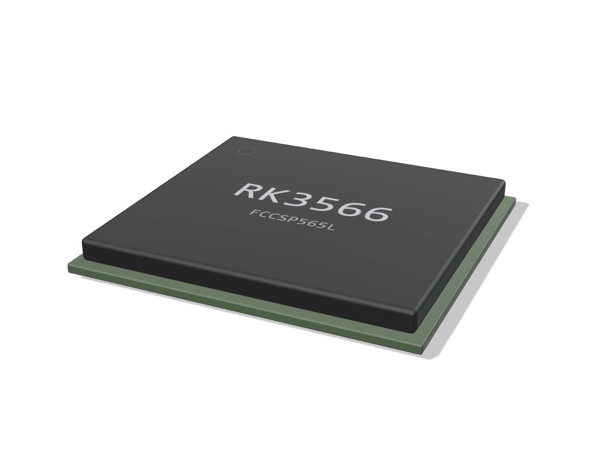
- CPU
- 4x A55 1.8 GHz
- GPU
- Mali-G52 2EE
- NPU
- 1 TOPS (INT8/INT16/FP16)
- Video
- 4K60 H.265/VP9/H.264 decode, 1080p60 H.265/H.264 encode
- PCIe
- PCIe 2.1 x1 (shared with SATA)
What the RK3566 is for
Right for
- Cost-driven Linux HMI and kiosk boards: one 4K60 HDMI 2.0 output or an eDP, MIPI DSI or LVDS panel, with a Mali-G52 that runs on mainline Panfrost
- E-paper devices: the SoC has an on-chip EBC e-ink panel interface (Pine64 PineNote is built on it)
- Raspberry Pi CM4 footprint replacements: SOQuartz, Luckfox Core3566 and BIGTREETECH CB2 all put an RK3566 on CM4-style 2x 100-pin connectors
- Handhelds and battery products: RK817-5 pairing adds a charger and audio codec, and Anbernic and Powkiddy handhelds have mainline device trees
- Single-port network or storage boxes: one GbE MAC plus a PCIe 2.1 x1 lane for a second NIC or NVMe (NanoPi R3S adds a PCIe GbE controller)
Wrong for
- Designs needing PCIe Gen3 or more than one lane: there is a single PCIe 2.1 x1 root port, and it shares its PHY with SATA
- Two independent displays: the datasheet allows two simultaneous outputs only from the same source; Rockchip lists single display output
- Two Ethernet ports on MACs, DDR ECC or CAN: all three are RK3568 features, not RK3566
- Products that need hardware HEVC/VP9 decode or the NPU on mainline Linux today: neither driver supports RK3566 as of 7.3-rc7
- Encode above 1080p60 or any 4K encode
Cost and constraints
- SerDes is shared: USB 3.0 host or SATA1 on one PHY, PCIe 2.1 or SATA2 on the other, so lane functions are fixed at schematic time
- FCCSP565L, 15.5 x 14.4 mm, mixed 0.65 mm and 0.4 mm ball pitch with 0.25 mm balls: plan via and fanout rules before committing to a stackup
- BOM is the SoC (USD 9.84 at 102 pieces on LCSC), an RK809-5 or RK817-5 PMIC, a separate VDD_CPU buck (TCS4525 on every Pine64 and Radxa schematic checked) and 32-bit LPDDR4/4X
- DRAM ceiling is 8 GB on one 32-bit channel; Rockchip publishes RK3566 DDR init binaries at 920 and 1056 MHz only
- Rated 0 to 80 C ambient; no extended-temperature RK3566 appears in the order tables
Inside the RK3566
Drawn by Groundplane from the datasheet rev 1.4. Not Rockchip artwork.
- 32-bit DDR3/DDR4/LPDDR4/4X
- eMMC 5.1
- SD 3.0 / SDIO 3.0
- FSPI NOR or NAND
- 8-bit parallel NAND
- 4x Cortex-A55 up to 1.8 GHz
- 32 KB L1 I/D per core
- 512 KB shared L3
- Neon, FPU, crypto extensions
- Mali-G52 2EE up to 800 MHz
- 2D graphics engine (RGA)
- 1 TOPS INT8/INT16/FP16
- 4K60 H.265/H.264/VP9 decoder
- 1080p60 H.264/H.265 encoder
- JPEG codec
- IEP deinterlacer
- 32-bit DDR controller
- DDR3/DDR4/LPDDR3/LPDDR4/4X
- 64 KB SRAM, 32 KB BootROM
- VOP, 2 outputs, same source
- HDMI 2.0 and eDP 1.3 TX
- Dual MIPI DSI or LVDS
- EBC e-ink controller
- MIPI CSI-2 RX, 4 lanes
- 16-bit DVP
- 8 MP ISP
- TrustZone, secure boot
- Crypto engine, TRNG
- 8 Kbit OTP
- PMU, 5 voltage domains
- RISC-V MCU, mailbox
- 2x DMAC, timers, watchdog
- TSADC x2, SARADC x4
- PCIe 2.1 x1 or SATA
- USB 3.0 host or SATA
- 2x USB 2.0 host
- USB 2.0 OTG
- GbE MAC (RGMII)
- HDMI 2.0, eDP 1.3
- 2x MIPI DSI / LVDS
- MIPI CSI-2 x4, DVP
- I2S/TDM, PDM, SPDIF
- UART x10, I2C x6, SPI x4, PWM x16
Read from the documents
Each value names the document it was read from.
| CPU | 4x Cortex-A55, 32 KB L1 I/D each, 512 KB L3, ARMv8 crypto extensions; up to 1.8 GHz | Datasheet Rev 1.4, 1.2.1, Table 3-2 |
|---|---|---|
| GPU | Mali-G52 1-Core-2EE up to 800 MHz; OpenGL ES 1.1/2.0/3.2, Vulkan 1.0/1.1, OpenCL 2.0 Full Profile | Datasheet Rev 1.4, 1.2.10, Table 3-2 |
| NPU | Up to 1 TOPS, INT8/INT16/FP16/BFP16, up to 1.0 GHz (Rev 1.0 and 1.1 stated 0.8 TOPS, INT8/INT16) | Datasheet Rev 1.4, 1.2.2, Table 3-2 |
| Video decode | H.265 Main10, H.264 and VP9 Profile 0/2 up to 4096x2304 at 60 fps; VP8, VC-1, MPEG-4, MPEG-2, MPEG-1 up to 1920x1088 at 60 fps; JPEG decode 1080p120 | Datasheet Rev 1.4, 1.2.7, 1.2.8 |
| Video encode | H.264 and H.265 up to 1920x1080 at 60 fps (H.265 4096x4096 at 10 fps with tiles); JPEG encode up to 8192x8192 | Datasheet Rev 1.5, 1.2.7, 1.2.8 |
| Memory | 32-bit DDR3, DDR3L, DDR4, LPDDR3, LPDDR4, LPDDR4X, each up to 2133; 8 GB max; 2 ranks (DDR3/DDR4) or 4 ranks (LPDDR) | Datasheet Rev 1.4, 1.2.5 |
| Storage | eMMC 5.1 HS200 with CMD queue, SD 3.0, SDIO 3.0, FSPI NOR/NAND (1/2/4-bit), 8-bit parallel NAND with 70-bit/1 KB ECC | Datasheet Rev 1.4, 1.2.5, 1.2.15 |
| Display | HDMI 2.0 TX up to 4096x2304 at 60 Hz with HDCP 1.4/2.2; eDP 1.3 x4 up to 2560x1600 at 60 Hz; 2x MIPI DSI x4 (1080p60 single, 2560x1600 at 60 Hz dual); LVDS shared with DSI0; BT.656/BT.1120; EBC e-ink. Two simultaneous outputs from the same source | Datasheet Rev 1.4, 1.2.12, 1.2.13 |
| Camera | MIPI CSI-2 RX, 4 lanes or 2x 2 lanes at up to 2.5 Gbps per lane; 16-bit DVP; ISP up to 4096x2304 with 3A, HDR merge, 2D/3D NR | Datasheet Rev 1.4, 1.2.11 |
| PCIe | 1x PCIe 2.1 x1 (5 GT/s), root complex only; shares its PHY with SATA2 | Datasheet Rev 1.4, 1.2.15 Multi-PHY |
| USB | 1x USB 3.0 host (shares its PHY with SATA1), 2x USB 2.0 host, 1x USB 2.0 OTG (also the maskrom download port) | Datasheet Rev 1.4, 1.2.4, 1.2.15 |
| Ethernet | 1x GMAC, 10/100/1000 RGMII or 10/100 RMII, TSO/UFO offload | Datasheet Rev 1.4, 1.2.15 |
| SATA | Up to 2x SATA 3.0 (6 Gbps), each on a PHY shared with USB 3.0 host or PCIe | Datasheet Rev 1.4, 1.2.15 Multi-PHY |
| Other I/O | 10x UART, 6x I2C, 4x SPI, 16x PWM, 2x 8-ch I2S/TDM (one for HDMI), 2x 2-ch I2S, 8-ch PDM, SPDIF, 4-ch 10-bit SARADC, 2x TSADC, ISO7816, GPIO x142 | Datasheet Rev 1.4, 1.2.14 to 1.2.16, 1.3 |
| Package | FCCSP565L, 15.5 x 14.4 mm, ball pitch 0.65 mm and 0.4 mm, 0.25 mm balls, SnAgCu, MSL3 | Datasheet Rev 1.4, 1.2.16, 2.4, 2.5 |
| Operating range | Ambient 0 to 80 C; Tj max 125 C; theta-JA 20.7, theta-JB 17.7, theta-JC 1.5 C/W (JEDEC 4-layer board) | Datasheet Rev 1.4, Table 3-1, Table 3-2, Table 4-1 |
Variants
| RK3566 | Base part: quad A55 to 1.8 GHz, GPU to 800 MHz, NPU to 1.0 GHz (1 TOPS), FCCSP565L. | Datasheet Rev 1.4 |
|---|---|---|
| RK3566-D | Separate ordering code in the Rev 1.4 order table, described as the RK3566 "with the Dolby function"; same FCCSP565L package. Rev 1.5 (2024-12-11) deletes RK3566-D from the order table, leaving only RK3566. | Datasheet Rev 1.5 |
| RK3566T | Lower-binned RK3566 used on Pine64 Quartz64 Zero and, per the kernel commit, Radxa ROCK 3C and ZERO 3W/3E: fewer CPU and GPU OPPs and no functional NPU. Mainline caps the CPU at 1.416 GHz and the GPU at 700 MHz because the vendor kernel OPP tables stop at 1.4 GHz, while board vendors advertise 1.6 GHz. No Rockchip datasheet for RK3566T was found. | Other |
| RK3568 (sibling) | Same CPU, GPU, NPU and VPU but a different package (FCBGA636L, 19 x 19 mm, 0.65 mm pitch), so not pin compatible. Adds PCIe 3.0 x2 (or two x1) beside PCIe 2.1, a second GMAC, USB 3.0 OTG, a third SATA port, three simultaneous displays, DDR3/DDR4 ECC and 3x CAN. | Datasheet Rev 1.0 |
What to watch when you design with it
Power and PMIC
Every public RK3566 schematic checked uses a Rockchip PMIC plus a separate I2C buck for the CPU rail: Quartz64 Model A, Quartz64 Zero and Radxa CM3 use RK817-5 (charger and audio codec on chip), Quartz64 Model B, SOQuartz and ROCK 3C use RK809-5 (no charger, codec on chip), and all of them put VDD_CPU on a TCS4525 buck with a remote feedback line from the SoC. Rockchip's own brief shows RK817-5 in its reference application. RK809 provides five bucks (2.5 A, 2.5 A, 1.5 A, 1.5 A, 2.5 A) and nine LDOs. Core rails (CPU, GPU, NPU, logic) are 0.9 V typical; I/O banks run at 3.3 V or 1.8 V and the datasheet warns that GPIO bank configuration must match the actual supply or the pins can be overvoltage-damaged.
Sources: Board schematic v2.0, Board schematic v1.1, Board schematic V1.400, Product brief, PMIC Rev 1.01, PMIC Rev 2.1, Datasheet Rev 1.4
DDR
One 32-bit channel, 8 GB maximum. Rev 1.4 of the datasheet lists DDR3, DDR3L, LPDDR3, DDR4, LPDDR4 and LPDDR4X at up to 2133; LPDDR4X needs a separate 0.6 V VDDQL rail in addition to the 1.1 V VDDQ. Every public RK3566 schematic checked (Quartz64 A, B and Zero, SOQuartz, ROCK 3C, CM3) uses LPDDR4 or LPDDR4X. DRAM training is a closed binary: rockchip-linux/rkbin ships RK3566 DDR init images at 920 MHz and 1056 MHz only, against up to 1560 MHz for RK3568, and mainline U-Boot loads that blob as ROCKCHIP_TPL. Byte and DQ swap rules for each DRAM type live in the Rockchip hardware design guide, which we could not find on a linkable host; copy a vendor layout or ask your Rockchip FAE before swapping lanes.
Sources: Datasheet Rev 1.4, github.com, github.com
High-speed interfaces
Two combo PHYs carry all the SerDes: PHY1 is USB 3.0 host or SATA1, PHY2 is PCIe 2.1 x1 or SATA2. Boards resolve the conflict differently: Quartz64 Model A brings out PCIe and SATA, ODROID-M1S and ROCK 3C put PCIe on M.2 or an FPC, Orange Pi 3B wires its M.2 slot for either NVMe or SATA. The datasheet calls for 75 to 200 nF AC coupling on USB 3.0 and PCIe and 6 to 12 nF on SATA. There is one GMAC, so a second Ethernet port has to come from PCIe or USB (NanoPi R3S uses an RTL8111H on PCIe).
Sources: Datasheet Rev 1.4, Board schematic v2.0, friendlyelec.com
Boot and maskrom
The BootROM boots from FSPI flash, NAND, eMMC or SD and falls back to USB download on the USB 2.0 OTG port (maskrom). The Quartz64 Model A schematic documents the two ways in: short eMMC_D0 to ground (eMMC or NAND) or short FSPI_CLK to ground (SPI flash) while powering up, and recommends reserving those test points. It also documents the FLASH_VOL_SEL strap (GPIO0_A7): low means VCCIO2, the flash I/O bank, is 3.3 V; high means 1.8 V. The strap must match the rail. Vendors add a dedicated MASK button (NanoPi R3S) or a maskrom key (Orange Pi CM4 base board).
Sources: Datasheet Rev 1.4, Board schematic v2.0, wiki.friendlyelec.com
Thermal
Datasheet thermal resistance is theta-JA 20.7 C/W, theta-JB 17.7 C/W and theta-JC 1.5 C/W on a JEDEC 4-layer 114.3 x 101.6 mm board, with Tj max 125 C and an ambient rating of 0 to 80 C. Pine64 markets the Quartz64 Zero (RK3566T) as running without a heatsink under sustained load; Hardkernel ships the ODROID-M1S with a heatsink. Two on-chip temperature sensors and a TSADC_SHUT output are available for a hardware thermal reset.
Sources: Datasheet Rev 1.4, pine64.com
Gotchas
Check which part is on the board you copy: the kernel identifies Radxa ROCK 3C and ZERO 3W/3E as RK3566T (no usable NPU, lower OPPs), and their schematics are therefore not a reference for NPU power. Dual-display products need RK3568: RK3566 drives two outputs only from the same source. LVDS is unavailable when both DSI ports are in dual-MIPI mode. The NPU rating moved from 0.8 TOPS (Rev 1.0 and 1.1) to 1 TOPS (Rev 1.2 onward); several vendor pages still quote 0.8.
Sources: Other, Datasheet Rev 1.4, Datasheet Rev 1.0
Layout guides for the RK3566's interfaces
Public layout guidance for each interface this chip has, from vendors who publish it, plus our calculators.
LPDDR4
Point-to-point routing; TI notes that on-die termination on both ends means no board termination is needed. Byte lanes length-matched to their strobe and command/address matched to the clock, all over a solid reference plane. Impedance targets differ by vendor: TI AM62x and ADI EE-480 use 40 ohm single-ended and 80 ohm differential, Synaptics SL1680 uses 50 and 85 ohm, AMD Versal 45 and 82 ohm. Use the SoC vendor's own target and simulate.
- AM62x, AM62Lx DDR Board Design and Layout GuidelinesTexas Instruments, SPRAD06, C, 2025
- AM62Ax, AM62Px, AM62Dx LPDDR4 Board Design and Layout GuidelinesTexas Instruments, SPRAD66, B, 2024
- ADSP-2184x/ADSP-SC84x LPDDR4 Board Design GuidelinesAnalog Devices, EE-480, 1, 2026
- SL1680 General PCB Design and LPDDR4 & LPDDR4(x) Interface Layout GuidelinesSynaptics, PN 506-001390-01, E
- DDR length matching calculatorGroundplane calculator
LPDDR4X
Same topology and matching discipline as LPDDR4, with a lower I/O voltage, so routing rules are usually published for both together. Synaptics SL1680 gives 50 ohm single-ended and 85 ohm differential for LPDDR4 and LPDDR4X; AMD Versal gives 45 and 82 ohm. Check the SoC vendor target before fixing the stackup.
- SL1680 General PCB Design and LPDDR4 & LPDDR4(x) Interface Layout GuidelinesSynaptics, PN 506-001390-01, E
- SL1640 General PCB Design and DDR4 & LPDDR4(x) Interface Layout GuidelinesSynaptics, PN 506-001529-01, D
- Versal Adaptive SoC PCB Design User Guide: PCB Routing Guidelines for LPDDR4/4x InterfacesAMD, UG863, 1.12, 2026
- DDR length matching calculatorGroundplane calculator
DDR4
DDR4 uses pseudo open-drain data signaling and needs a VPP supply, with command/address routed fly-by or as a balanced tree depending on device count. TI AM62x uses 40 ohm single-ended and 80 ohm differential; AMD Versal uses 50 and 90 ohm, relaxed under the BGA. Match data to strobe per byte and command/address to clock.
- AM62x, AM62Lx DDR Board Design and Layout GuidelinesTexas Instruments, SPRAD06, C, 2025
- Versal Adaptive SoC PCB Design User Guide: PCB Routing Guidelines for DDR4 InterfacesAMD, UG863, 1.12, 2026
- SL1640 General PCB Design and DDR4 & LPDDR4(x) Interface Layout GuidelinesSynaptics, PN 506-001529-01, D
- PCB Design Guidelines (HSSI, EMIF, MIPI, True Differential, PDN) User Guide: Agilex 5 FPGAs and SoCsAltera, 821801, 2026
- DDR length matching calculatorGroundplane calculator
- Via current calculatorGroundplane calculator
DDR3 / DDR3L
Fly-by command/address with termination at the end of the chain, point-to-point data lanes matched to their strobe, and a clean VREF. ST recommends 55 ohm single-ended and 100 ohm differential for DDR3 and DDR3L on STM32MP1 boards, and shows that a 4-layer board is possible with strict layer allocation.
- STM32MP1 Series DDR memory routing guidelinesSTMicroelectronics, AN5122, 3, 2019
- DDR3 Design Requirements for KeyStone DevicesTexas Instruments, SPRABI1, D, 2022
- SL2610 General PCB Design and DDR3L/DDR4 & LPDDR4(x) Interface Layout GuidelinesSynaptics, PN 506-001629-01, A, 2025
- DDR length matching calculatorGroundplane calculator
LPDDR3
Point-to-point and normally unterminated, with command/address matched to the clock and each byte matched to its strobe. ST gives the same targets for LPDDR3 as for DDR3: 55 ohm single-ended and 100 ohm differential. Few current public guides cover LPDDR3, so treat the SoC vendor's reference layout as the stronger source.
- STM32MP1 Series DDR memory routing guidelinesSTMicroelectronics, AN5122, 3, 2019
- DDR length matching calculatorGroundplane calculator
eMMC
A single-ended bus: CLK, CMD, DAT0 to DAT7 and, for HS400, the data strobe. TI and Synaptics both route it at 50 ohm single-ended, match the group, and keep stubs short; Synaptics places a 22 or 33 ohm series resistor on CLK and STRB. At HS400 TI also checks the eMMC I/O supply impedance, not just the traces.
- AM62Px eMMC HS400 Board Design and Simulation GuidelinesTexas Instruments, SPRADP5, A, 2026
- Astra Machina Foundation Series eMMC ConfigurationSynaptics, PN 506-001594-01, D
- i.MX28 Layout and Design GuidelinesNXP (Freescale), AN4215, 0, 2010
SD card / SDIO
Single-ended CLK, CMD and four data lines over a solid ground plane, at constant trace width and matched length. NXP asks for clock-to-neighbor spacing greater than twice the trace height above the plane and 1.5 times for data and CMD, with 45 degree bends. UHS modes switch the I/O to 1.8 V, so a level translator often sits next to the socket.
- NVT4557/NVT4558/NVT4858 voltage-level translator layout guidelineNXP, AN13158, 1.1, 2022
- i.MX28 Layout and Design GuidelinesNXP (Freescale), AN4215, 0, 2010
- SD Physical Layer Simplified SpecificationSD Association, 9.10, 2023
PCIe
AC-coupled differential lanes routed with no stubs, minimal vias and back-drilled or blind vias where speed demands, with lane-to-lane skew handled by the receiver. Targets differ by guide: TI Jacinto 7 uses 85 ohm differential for lanes and 100 ohm for the reference clock, while TI's earlier SoC guide tabulates 100 ohm and, for some devices, 95 ohm. Match the target to your connector and stackup.
- Jacinto7 AM6x, TDA4x, and DRA8x High-Speed Interface Design GuidelinesTexas Instruments, SPRACP4, A, 2024
- High-Speed Interface Layout GuidelinesTexas Instruments, SPRAAR7, J, 2023
USB 3.x
SuperSpeed TX and RX pairs are routed at 90 ohm differential in all three TI guides (SPRAAR7 lists 95 ohm for some devices), with AC coupling capacitors on TX, symmetric pad and via placement, and matched via counts within each pair. Keep the pairs away from the USB 2.0 pair and other aggressors, and place ESD at the connector.
- High-Speed Layout Guidelines for Signal Conditioners and USB HubsTexas Instruments, SLLA414, A, 2026
- Jacinto7 AM6x, TDA4x, and DRA8x High-Speed Interface Design GuidelinesTexas Instruments, SPRACP4, A, 2024
- High-Speed Interface Layout GuidelinesTexas Instruments, SPRAAR7, J, 2023
USB 2.0
One D+/D- pair at 90 ohm differential, routed in parallel for its whole length with minimal deviations at the connector and package. NXP keeps clocks and periodic signals at least 50 mils away and other signals at least 20 mils away from the pair.
- High-Speed Layout Guidelines for Signal Conditioners and USB HubsTexas Instruments, SLLA414, A, 2026
- High-Speed Interface Layout GuidelinesTexas Instruments, SPRAAR7, J, 2023
- i.MX28 Layout and Design GuidelinesNXP (Freescale), AN4215, 0, 2010
HDMI
Four TMDS pairs (three data, one clock) at 100 ohm differential, as both TI guides state, with tight intra-pair matching and as few vias as possible between the SoC and the connector. HDMI also needs 5 V supply switching, DDC and CEC level handling, hot-plug detect and ESD at the connector.
- High-Speed Layout Guidelines for Signal Conditioners and USB HubsTexas Instruments, SLLA414, A, 2026
- High-Speed Interface Layout GuidelinesTexas Instruments, SPRAAR7, J, 2023
- TPD12S016 PCB Layout Guidelines for HDMI ESDTexas Instruments, SLLA324, 2012
DisplayPort / eDP
Main-link lanes are routed at 100 ohm differential in both TI guides, with no stubs and few vias; TI Jacinto 7 allows 2 vias per trace. When DisplayPort shares a USB-C connector through alt mode, the lanes run through the Type-C mux and the SuperSpeed rules apply to the shared path.
- High-Speed Layout Guidelines for Signal Conditioners and USB HubsTexas Instruments, SLLA414, A, 2026
- Jacinto7 AM6x, TDA4x, and DRA8x High-Speed Interface Design GuidelinesTexas Instruments, SPRACP4, A, 2024
MIPI DSI
MIPI D-PHY clock and data lanes are routed as 100 ohm differential pairs over a solid reference; TI Jacinto 7 allows no stubs, 2 vias per trace and 40 ps lane-to-lane skew. Connectors and flex cables to the panel are usually the largest discontinuity, so keep the board segment short and clean.
- Jacinto7 AM6x, TDA4x, and DRA8x High-Speed Interface Design GuidelinesTexas Instruments, SPRACP4, A, 2024
- PCB Design Guidelines (HSSI, EMIF, MIPI, True Differential, PDN) User Guide: Agilex 5 FPGAs and SoCsAltera, 821801, 2026
MIPI CSI-2
Same D-PHY rules as DSI: 100 ohm differential lanes in both TI guides, with lane-to-lane skew bounded (40 ps in TI Jacinto 7). Size the lane count and lane rate from the sensor's output format before routing.
- Jacinto7 AM6x, TDA4x, and DRA8x High-Speed Interface Design GuidelinesTexas Instruments, SPRACP4, A, 2024
- High-Speed Interface Layout GuidelinesTexas Instruments, SPRAAR7, J, 2023
- PCB Design Guidelines (HSSI, EMIF, MIPI, True Differential, PDN) User Guide: Agilex 5 FPGAs and SoCsAltera, 821801, 2026
- MIPI CSI-2 bandwidth calculatorGroundplane calculator
LVDS
Tightly coupled differential pairs terminated at the receiver in 100 ohm, with TI's EMI guide asking for 100 ohm differential traces within 5 percent. Keep pairs matched and away from other aggressors, and avoid stubs and reference plane gaps along the route to the panel connector.
- LVDS Owner's Manual: Including High-Speed CML and Signal ConditioningTexas Instruments, SNLA187, 4th edition, 2008
- High-Speed Layout Guidelines for Reducing EMI for LVDS SerDes DesignsTexas Instruments, SNLA302, 2018
- LVDS SerDes Gen I PCB and Interconnect Design-In GuidelinesTexas Instruments, SNLA008, A, 2018
Ethernet (RGMII / RMII)
TI routes MAC-to-PHY (MII family) traces at 50 ohm single-ended, under 6 inches, matched within 20 mils for gigabit, and the PHY-side MDI pairs at 100 ohm differential. RGMII also needs a 1.5 to 2.0 ns clock-to-data delay, added on the board or inside the MAC or PHY (RGMII-ID); decide which before layout so it is not applied twice.
- Ethernet PHY PCB Design Layout ChecklistTexas Instruments, SNLA387, 2021
- PCB Design Guideline for RGMII InterfaceRenesas, R01AN6272EJ0141, 1.41, 2026
- i.MX28 Layout and Design GuidelinesNXP (Freescale), AN4215, 0, 2010
SATA
AC-coupled TX and RX pairs at 100 ohm differential in TI's SoC guide, routed with the same via, stub and reference plane rules as PCIe and USB 3. On Rockchip parts SATA usually shares a combo PHY with PCIe or USB 3, so the lane is routed once to whichever connector the design picks.
- High-Speed Interface Layout GuidelinesTexas Instruments, SPRAAR7, J, 2023
- High-Speed Layout Guidelines for Signal Conditioners and USB HubsTexas Instruments, SLLA414, A, 2026
Board-level design guides
Impedance and timing, power, thermal and ESD guidance that applies to any board around this chip.
Impedance and timing
Every high-speed interface on the board comes down to the same two numbers: the trace impedance your stackup actually gives, and the delay each trace adds. Set the stackup with your fab first, then route to its impedance table and match lengths in time, not millimeters, where the layers differ.
- High-Speed Interface Layout GuidelinesTexas Instruments, SPRAAR7, J, 2023
- PCB impedance calculatorGroundplane calculator
- PCB propagation delay calculatorGroundplane calculator
Power delivery
For each switching regulator, place and route the input capacitor first, keep the switching current loop small, and keep the switch node short. Give the SoC rails solid planes and decoupling at the balls, and size current-carrying copper and vias for the real load.
- Five steps to a great PCB layout for a step-down converterTexas Instruments, SLYT614, 2015
- AN-1149 Layout Guidelines for Switching Power SuppliesTexas Instruments, SNVA021, C, 2013
- AN-1229 SIMPLE SWITCHER PCB Layout GuidelinesTexas Instruments, SNVA054, C, 2013
- Buck converter calculatorGroundplane calculator
- LDO power dissipation calculatorGroundplane calculator
- PCB trace width calculatorGroundplane calculator
- Via current calculatorGroundplane calculator
Thermal
Theta-JA is measured on a JEDEC test board that carries most of the heat, so it does not transfer directly to a product board; use it to compare packages and use the psi metrics for estimates. Thermal vias under the package, copper area and copper thickness move the most heat into the board.
- Semiconductor and IC Package Thermal MetricsTexas Instruments, SPRA953, D, 2024
- AN-2020 Thermal Design By Insight, Not HindsightTexas Instruments, SNVA419, C, 2013
- Heatsink thermal resistance calculatorGroundplane calculator
- LDO power dissipation calculatorGroundplane calculator
ESD protection
Place the TVS as close to the connector as design rules allow, route from the connector to the TVS with no stub, and keep the protected IC further from the TVS than the TVS is from the connector. Choose parts by clamping performance and by capacitance low enough for the interface speed.
- ESD Protection Layout GuideTexas Instruments, SLVA680, A, 2022
- Reading and Understanding an ESD Protection Data SheetTexas Instruments, SLLA305, A
- TPD12S016 PCB Layout Guidelines for HDMI ESDTexas Instruments, SLLA324, 2012
- PCB conductor spacing calculator (IPC-2221)Groundplane calculator
Rockchip's hardware design guide
Rockchip's hardware design guide, EVB reference schematics and DDR templates come from Rockchip or an authorized agent, usually under NDA, or through your SoM vendor. We do not link copies circulating elsewhere. The vendor schematics and open designs on the Boards tab are real, shipped layouts on the RK3566 and the best public reference.
BSP, mainline and toolkits
| Area | Status | Links |
|---|---|---|
| Vendor BSP kernel | Rockchip maintains develop-5.10, develop-6.1, develop-6.6 and develop-6.12 branches; develop-6.12 is at 6.12.69 and carries 53 RK3566 board device trees. This is the kernel the NPU, rkvdec2 and ISP drivers need.Checked 2026-10-13 | |
| Mainline Linux | SoC dtsi and Quartz64 Model A landed in 5.16; GPU node for Panfrost (Mali-G52) in 5.18; USB 3.0 and SATA via the combo PHY in 5.19; VOP2 display, HDMI and PCIe in 6.0; MIPI DSI, the Hantro decoder (H.264, VP8, MPEG-2) and JPEG encoder in 6.1; RGA in 6.5; the RK3566T dtsi in 6.13; VICAP camera capture in 6.19. Not upstream as of 7.3-rc7: HEVC/VP9 decode (rkvdec has no RK3566/RK3568 compatible), the NPU (the rocket driver supports RK3588 only), and the ISP.Checked 2026-10-13 | |
| U-Boot | Mainline U-Boot supports RK3566 since v2023.04 (Radxa CM3 IO board); the current board list has 15 RK3566 targets including Quartz64 A/B, SOQuartz, ROCK 3C, ZERO 3, CM3 IO, Orange Pi 3B, ODROID-M1S, NanoPi R3S and TaishanPi. BL31 can be open TF-A (plat/rockchip/rk3568); DRAM init is still the rkbin binary. Rockchip's own fork is rockchip-linux/u-boot (next-dev).Checked 2026-10-13 | |
| NPU toolkit | RKNN-Toolkit2 lists the RK3566/RK3568 series as a supported platform; the README names v2.5.0 as the latest version (last GitHub release tag v2.3.2, 2025-04-09). Runs on the vendor kernel RKNPU driver only.Checked 2026-10-13 | |
| Video (MPP) | Rockchip MPP (latest tag 1.1.0) drives the full VPU, including 4K HEVC/VP9 decode, on the vendor kernel. Mainline only has the Hantro H.264/VP8/MPEG-2 decoder and JPEG encoder for this SoC.Checked 2026-10-13 | |
| 2D (RGA) | librga (vendor; latest tagged release v1.10.0, source at 1.10.6). The RGA node has been in the mainline device tree since 6.5.Checked 2026-10-13 | |
| Android | Vendor images only: Radxa publishes Android 11 and Android 14 images for ROCK 3C; Orange Pi lists Android 11 for the 3B; Boardcon lists Android 14 for CM3566 and Compact3566.Checked 2026-10-13 | |
| Distributions | Armbian has board pages for Quartz64 A and B, Radxa ZERO 3, ROCK 3C, Orange Pi 3B, ODROID-M1S and NanoPi R3S. Radxa ships Radxa OS (Debian) images; Orange Pi ships Ubuntu and Debian. Handhelds have mainline device trees: the first Anbernic RG353 boards from 6.1, the Powkiddy RGB30, RK2023 and X55 in later releases.Checked 2026-10-13 | |
| Community | Pine64 documentation and forum (Quartz64, SOQuartz, PineNote), Radxa forum, FriendlyELEC wiki.Checked 2026-10-13 |
RK3566 on GitHub
Repositories for this chip: vendor code, mainline work, toolkits, distributions and open hardware.
- Kernelrockchip-linux/kernelRockchip BSP kernel; RK3566 shares the rk3568 dtsi and is supported on develop-4.19, develop-5.10 and develop-6.1. Last commit 2026-08.
- Kerneldreemurrs-embedded/linux-pinetab2Mainline kernel with patches for the RK3566 PineTab2 tablet. Last commit 2025-06.
- Kerneltorvalds/linuxMainline Linux has about 55 RK3566 device trees, including PineTab2, Quartz64 and the Anbernic handhelds. Last commit 2026-10.
- Bootloaderrockchip-linux/u-bootRockchip U-Boot; next-dev rk3568 SoC code is used for RK3566 as well. Last commit 2026-08.
- Bootloaderrockchip-linux/rkbinDDR init, loaders and BL31; RK3566 boots with the rk3568 and rk356x binaries in bin/rk35. Last commit 2026-08.
- Bootloaderu-boot/u-bootMainline U-Boot has RK3566 board configs such as Anbernic RGxx3, NanoPi R3S and LCKFB Taishanpi on the rk3568 SoC code. Last commit 2026-10.
- BootloaderTrustedFirmware-A/trusted-firmware-aRead-only mirror of TF-A; plat/rockchip/rk3568 provides the open BL31 that RK3566 boards use. Last commit 2026-10.
- Bootloaderjaredmcneill/quartz64_uefiEDK2 UEFI firmware started on the RK3566 Quartz64 and now covering several RK3566 and RK3568 boards. Last commit 2026-06.
- NPUairockchip/rknn-toolkit2RKNN-Toolkit2 converter and RKNPU2 runtime; RK3566 has the same 1 TOPS NPU as RK3568. RKLLM does not support it. Last commit 2026-10.
- NPUairockchip/rknn_model_zooReference model conversions and C demos with RK3566 listed for every vision model. Last commit 2026-10.
- Mediarockchip-linux/mppMedia Process Platform; RK3566 is listed in the README for hardware decode and encode. Last commit 2026-09.
- Mediaairockchip/librgaRGA 2D acceleration library with RK3566 in its supported chip list. Last commit 2026-06.
- Distributionarmbian/buildArmbian build framework with RK3566 boards such as Radxa ZERO 3, Orange Pi 3B, BigTreeTech CB2 and several TV boxes. Last commit 2026-10.
- DistributionJoshua-Riek/ubuntu-rockchipUbuntu images that include Radxa ZERO 3 and Orange Pi 3B on RK3566; archived in 2025. Archived. Last commit 2025-09.
- DistributionROCKNIX/distributionHandheld gaming distribution with a dedicated RK3566 device for handhelds such as the Anbernic RG353 series. Last commit 2026-10.
- Open hardwareradxa/radxa-som-projectsRadxa reference carrier designs in Altium; the cm3 and cm3s folders are RK3566 modules. Last commit 2026-09.
- Open hardwarehw-myry/rk3566-devkitPersonal 6 layer RK3566 board with LPDDR4 in Altium, including PCB, schematic sheets and pick and place files. Last commit 2026-03.
- KiCadtomek-szczesny/radxa-cm3-kicadKiCad symbol and footprint for the Radxa CM3 (RK3566) module. Last commit 2022-10.
- Toolsrockchip-linux/rkdeveloptoolRockchip open source USB flashing tool for maskrom and loader mode, the Linux and macOS alternative to RKDevTool. Last commit 2025-03.
- Communityblakeblackshear/frigateFrigate NVR RKNN detector lists rk3566 as a supported SoC. Last commit 2026-10.
RK3566 system on modules
Any of these can sit on a carrier board we design.
| Module | Vendor | Connector | RAM | Design files | Price | Buy |
|---|---|---|---|---|---|---|
| SOQuartz | Pine64 | Raspberry Pi CM4 form factor and connectors | 2, 4 or 8 GB LPDDR4 | Module schematic PDF (v1.1, 2021-08-16) and PCB placement PDF | USD 34.99 (Pine64 store, 2 GB, out of stock); USD 49.99 for 4 GB in stock | |
| CM3 | Radxa | 3x 100-pin 0.4 mm board-to-board | 1 to 8 GB LPDDR4 | Schematic PDFs (V1.31 to V1.322), placement maps, pinout XLSX, 3D STEP, connector footprint | ||
| CM3S | Radxa | 200-pin DDR2 SO-DIMM edge | Up to 8 GB LPDDR4 | Schematic PDFs (V1.5, V1.51), placement PDF, pinout XLSX, DXF | ||
| Orange Pi CM4 | Orange Pi | 2x 100-pin and 1x 24-pin board-to-board | 1 to 8 GB LPDDR4/4X | |||
| Core-3566JD4 | Firefly | 1, 2 or 4 GB (store variants) | USD 99 (Firefly store, 1 GB + 8 GB, out of stock); USD 139 for 2 GB + 32 GB in stock | |||
| Core3566 | Luckfox | Raspberry Pi CM4 compatible | 2 or 4 GB LPDDR4 | Module datasheet PDF and 3D model; no schematic found | USD 77.99 (Luckfox store, 2 GB, no eMMC, no Wi-Fi) | |
| CM3566 | Boardcon | 186-pin stamp-hole (castellated), 0.9 mm pitch | 1 to 8 GB | Hardware manual PDF and 3D model | ||
| PICO3566 | Boardcon | 200-pin SO-DIMM edge (Raspberry Pi CM3+ form factor) | 2 to 8 GB | Hardware manual PDF | ||
| MINI3566 | Boardcon | 3x 80-pin 0.5 mm board-to-board | 2 or 4 GB | Hardware manual, mechanical and interface connection PDFs | ||
| LubanCat 1CB / 1CF core boards, 1IOB / 1IOF carriers | Embedfire | Board-to-board (1CB) or gold finger (1CF) | LPDDR4/4X (options) | |||
| CB2 | BIGTREETECH | Raspberry Pi CM4 compatible, 2x 100-pin | 2 or 4 GB LPDDR4 | 3D STEP model and user manual on GitHub; no schematic |
Every public RK3566 board
| Board | Vendor | Type | RAM | Notable I/O | Design files | Price | Buy |
|---|---|---|---|---|---|---|---|
| Quartz64 Model A | Pine64 | SBC, 133 x 80 mm | 4 or 8 GB LPDDR4 | PCIe 2.1 x1 in open-ended x4 slot, SATA (early revisions only), USB 3.0 host, 3x USB 2.0, eDP, MIPI DSI, e-ink, CSI, GbE | Schematic PDF (v2.0, 2021-04-27) and connector placement PDF | USD 59.99 (Pine64 store, 4 GB) | |
| Quartz64 Model B | Pine64 | SBC, 85 x 56 mm | 4 or 8 GB LPDDR4 (store lists 4 GB) | M.2 (PCIe 2.1 x1), USB 3.0 host, 3x USB 2.0, GbE, HDMI, MIPI DSI, CSI | Schematic PDF (v1.3, 2022-01-24) and component placement PDF | USD 59.99 (Pine64 store, 4 GB) | |
| Quartz64 Zero (RK3566T) | Pine64 | SBC, 85 x 56 mm | 1 GB LPDDR4 (other capacities on commercial orders, MOQ 2000) | USB 3.0 host, Custom PCIe connector, HDMI 4Kp60, Wi-Fi 6, BT 5.4, 40-pin header | Schematic PDF (v0.1, 2024-04-28) and top/bottom placement PDFs | USD 19.99 (Pine64 store, 1 GB) | |
| SOQuartz Model-A Baseboard | Pine64 | Carrier | Schematic PDF and OrCAD DSN, PCB (Allegro Specctra export), Gerbers and drill, placement PDFs | USD 24.99 (Pine64 store) | |||
| SOQuartz Blade | Pine64 | Carrier | Schematic PDF, placement PDF, 1U rack STEP | USD 29.99 (Pine64 store) | |||
| PineNote | Pine64 | Dev kit, 10.3 inch e-ink tablet | EBC e-ink panel, TPS651851 e-paper PMIC, USB-C | Mainboard schematic PDFs (V1R1 2021-07-26, V1R2 2021-08-24), V1R1 placement PDF, USB-C board and USB-C console UART breakout schematic PDFs | USD 399 (Pine64 store, Community Edition, out of stock) | ||
| ROCK 3C | Radxa | SBC, 85 x 56 mm | 1, 2 or 4 GB LPDDR4 | USB 3.0 host, 2x USB 2.0, GbE (PoE with HAT), HDMI 1080p60, 2-lane DSI, PCIe 2.0 via M.2 extension board, 40-pin header | Schematic PDFs (V1.332, V1.400), placement PDFs, 2D DXF | USD 19.99 (Arace, 1 GB, out of stock); USD 44.90 for 2 GB in stock | |
| ZERO 3W | Radxa | SBC, Pi Zero class | 1 to 8 GB LPDDR4 | USB 3.0 host (Type-C), USB 2.0 OTG (Type-C), Micro HDMI, MIPI CSI, Wi-Fi 6, BT 5.4 | Schematic PDFs (V1.110, V1.12), 2D DXF, 3D STEP | USD 20.00 (Arace, 1 GB, no eMMC, out of stock); USD 39.99 for 2 GB in stock | |
| ZERO 3E | Radxa | SBC, Pi Zero class | 1 to 8 GB LPDDR4 | GbE (PoE with HAT), USB 3.0 host (Type-C), Micro HDMI, MIPI CSI | Schematic PDF (V1.200), placement map, 2D, 3D STEP | USD 30.99 (Arace, 4 GB; all variants out of stock) | |
| CM3 IO Board | Radxa | Carrier | HDMI, eDP, 2x DSI, PCIe 2.0, GbE, USB 3.0 | Full sources: Altium schematic and PCB, OrCAD DSN, PADS, BOM, DXF, STEP | USD 24.99 (Arace) | ||
| CM3S IO Board | Radxa | Carrier | HDMI, DSI, 2x MIPI CSI, SATA, PCIe 2.0, 100 Mbit Ethernet | Full sources: Altium schematic and PCB, OrCAD DSN, PADS, BOM, DXF | |||
| ODROID-M1S | Hardkernel | SBC, 90 x 65 mm | 2 GB (Lite), 4 or 8 GB LPDDR4 | M.2 M-key, PCIe 2.1 x1, 32 GB (Lite) or 64 GB eMMC on board, USB 3.0 host, GbE, HDMI 2.0, 4-lane DSI | USD 60 (Hardkernel store, M1S Lite 2 GB) | ||
| Orange Pi 3B | Orange Pi | SBC, 89 x 56 mm | 2, 4 or 8 GB LPDDR4/4X | M.2 M-key (PCIe 2.0 NVMe or SATA), eMMC socket, SPI flash, HDMI 2.0, eDP 1.3, DSI, GbE, USB 3.0 host | Schematic (Google Drive link on the vendor service page) | ||
| Orange Pi CM4 Base Board | Orange Pi | Carrier, 85 x 56 mm | M.2 M-key (NVMe or SATA), HDMI 2.0, eDP, DSI, 2x MIPI CSI, GbE, MaskROM key | ||||
| ROC-RK3566-PC | Firefly | SBC, 93.5 x 60.1 mm | 1 to 8 GB LPDDR4 | M.2 PCIe 2.1 NVMe (2242), USB 3.0, USB 2.0, GbE, HDMI 2.0, DSI, CSI | USD 119 (Firefly store, 1 GB + 8 GB, board only) | ||
| Station M2 | Firefly | SBC, Enclosed mini PC, 93.8 x 65.0 x 15.8 mm | 2, 4 or 8 GB LPDDR4 | M.2 PCIe 2.0 NVMe (2242), HDMI 2.0, GbE, USB 3.0, USB 2.0, Type-C OTG | USD 169 (Firefly store) | ||
| AIO-3566JD4 | Firefly | SBC | 1, 2 or 4 GB (store variants) | M.2 and SATA 3.0, GbE, Wi-Fi, 4G, 2x MIPI DSI, HDMI 2.0, eDP, 4-lane MIPI CSI | USD 149 (Firefly store, 1 GB + 8 GB, out of stock); USD 179 for 2 GB + 32 GB in stock | ||
| NanoPi R3S / R3S-LTS | FriendlyELEC | SBC, 57 x 57 mm (R3S) | 1 or 2 GB LPDDR4/4X | 2x GbE (RTL8211F native, RTL8111H on PCIe), USB 3.0 host, 0 or 32 GB eMMC, MASK button | Schematic PDFs (R3S 2406, R3S-LTS 2411) and 2D DXF | USD 38.00 (FriendlyELEC store, R3S-LTS 1 GB) | |
| Compact3566 | Boardcon | SBC, 85 x 56 mm | 2 to 8 GB | M.2, USB 3.0, 2x USB 2.0, GbE, HDMI, LVDS or DSI, CSI | Hardware manual and PCBA mechanical PDFs | ||
| EM3566 | Boardcon | SBC, 135 x 95 mm | 1 to 8 GB | RS485, USB 3.0, 4x USB 2.0, GbE, HDMI, DSI or LVDS, eDP, M.2 and mini PCIe | Hardware manual PDF | ||
| SBC3566 | Boardcon | SBC, 120 x 90 mm | 2 or 4 GB | RS485, M.2 (4G or NVMe), HDMI, LVDS, DSI, eDP, 2x MIPI CSI, GbE | |||
| KIT3566 | Boardcon | Dev kit, 140 x 110 mm | 2 to 8 GB | M.2 NVMe, mini PCIe 4G, 2x MIPI CSI, DSI, HDMI, GbE | |||
| LubanCat Zero N / Zero W | Embedfire | SBC | LPDDR4/4X (options) | GbE (Zero N) or Wi-Fi (Zero W), USB 2.0 host and OTG (Type-C), Optional eMMC | |||
| LubanCat 1 / 1N | Embedfire | SBC | LPDDR4/4X (options) | ||||
| SOM-3566-OSM with DB3566 evaluation board | Geniatech | Dev kit | Download behind an email form; contents not checked | ||||
| Tinker Board 3 | ASUS | SBC | 2 or 4 GB LPDDR4X | ||||
| TaishanPi (Taishan-RK3566) | LCKFB (LCSC) | SBC | Accessory boards (power, audio, case, expansion) published as open-source projects; main-board files not confirmed |
Prices and links as checked on the dates in our data; the latest check on this page was 2026-10-13. Amazon links marked * are affiliate links; see our disclosure.
Boards with published design files
| Project | Author | Files | Tool | License |
|---|---|---|---|---|
| Radxa CM3 IO Board (v1.330 and v1.360) | Radxa | Altium schematic and PCB project, OrCAD DSN, PADS ASCII and .pcb, Schematic PDF, BOM (v1.330), Placement PDF, DXF outlines, STEP (v1.360) | Altium | None stated in the repository |
| Radxa CM3S IO Board (v1.510) | Radxa | Altium schematic and PCB project, OrCAD DSN, PADS ASCII and .pcb, Schematic PDF, BOM, Placement PDF, DXF outline | Altium | None stated in the repository |
| Pine64 SOQuartz Model-A Baseboard (2022-05-22) | Pine64 | OrCAD schematic DSN, Schematic PDF, PCB as Specctra DSN exported from Allegro, Gerbers and drill (Allegro artwork, RAR), Top and bottom placement PDFs | OrCAD | None stated |
Buying the chip
The datasheet order table lists the RK3566 in trays of 1020 pieces. Module vendors (Pine64, Radxa, Boardcon, Firefly) sell SoMs, not bare chips; none publishes a bare-chip price. Pine64 states Quartz64 Zero supply is guaranteed until at least 2028.
- LCSC
- RK3566 (C2943786), BGA-565, 667 in stock; USD 14.65 at 1, 11.77 at 10, 10.74 at 30, 9.84 at 102 (tray of 102).
- Rockchip direct
- Rockchip lists service@rock-chips.com and regional offices; its contact page names Microtech (Suwon) and InSignal (Seoul) as official distributors for Korea. No other distributor list is published.
Datasheet, TRM and design documents
Linked where they are publicly hosted; we do not rehost Rockchip documents. These are third-party documents: we are not responsible for their accuracy, availability or confidentiality status. Disclosure.
- DatasheetRockchip RK3566 DatasheetRev 1.4 · 2024-06-21 · hosted by LCSC · checked 2026-10-13
- DatasheetRockchip RK3566 DatasheetRev 1.2 · 2022-09-30 · hosted by FriendlyELEC · checked 2026-10-13
- DatasheetRockchip RK3566 DatasheetRev 1.1 · 2021-03-05 · hosted by Luckfox · checked 2026-10-13
- DatasheetRockchip RK3566 DatasheetRev 1.0 · 2020-12-10 · hosted by Pine64 · checked 2026-10-13
- Product briefRK3566 Brief Datasheet2022 · hosted by Rockchip · checked 2026-10-13
- OtherRK3566 product pagehosted by Rockchip · checked 2026-10-13
- TRMRockchip RK3568 TRM Part 1 (covers RK3566)V1.1 · 2021-03-01 · hosted by Radxa · checked 2026-10-13
- TRMRockchip RK3568 TRM Part 2 (covers RK3566)V1.1 · 2021-03-01 · hosted by Radxa · checked 2026-10-13
- DatasheetRockchip RK3568 Datasheet (sibling, for comparison)Rev 1.0 · 2020-12-10 · hosted by Radxa · checked 2026-10-13
- PMICRockchip RK809 DatasheetRev 1.01 · 2018-08-28 · hosted by Radxa · checked 2026-10-13
- Board schematicPine64 Quartz64 Model A schematic (RK3566 + RK817-5 + TCS4525)v2.0 · 2021-04-27 · hosted by Pine64 · checked 2026-10-13
- Board schematicPine64 SOQuartz module schematic (RK3566 + RK809-5 + TCS4525)v1.1 · 2021-08-16 · hosted by Pine64 · checked 2026-10-13
- Board schematicRadxa ROCK 3C schematic (RK809-5 + TCS4525)V1.400 · hosted by Radxa · checked 2026-10-13
- OtherLinux commit: add SoC dtsi for the RK3566T variant2024-11-02 · hosted by kernel.org · checked 2026-10-13
- DatasheetRockchip RK3566 DatasheetRev 1.5 · 2024-12-11 · community mirror (rockchip.fr), not hosted by Rockchip · checked 2026-10-13
- TRMRockchip RK3568 TRM Part 1 (covers RK3566)V1.3 · 2022-09-30 · community mirror (rockchip.fr), not hosted by Rockchip · checked 2026-10-13
- PMICRockchip RK817 DatasheetRev 2.1 · 2023-03-20 · community mirror (rockchip.fr), not hosted by Rockchip · checked 2026-10-13
Questions about the RK3566
Yes. The WarpKVM 1080p main board is ours, on an RK3566: HDMI captured through a Rockchip RK628 HDMI-to-CSI bridge straight into the SoC, HDMI out, microSD boot, and Linux brought up on our bench.
The newest copy on a vendor or distributor host is Rev 1.4 (2024-06-21) on LCSC. FriendlyELEC hosts Rev 1.2, Luckfox Rev 1.1 and Pine64 Rev 1.0. Rev 1.5 (2024-12-11, removes the RK3566-D part number and rewords the encoder text) is only on the community mirror rockchip.fr, linked and labeled as a mirror. The TRM is shared with the RK3568 (Part 1 and Part 2 V1.1 on Radxa, Part 1 V1.3 on rockchip.fr).
Same CPU, GPU, NPU and video blocks. RK3568 adds PCIe 3.0 x2, a second GbE MAC, USB 3.0 OTG, a third SATA port, three independent displays, DDR ECC and CAN, in a larger 19 x 19 mm FCBGA636 package, so the two are not pin compatible. RK3566 keeps one PCIe 2.1 lane, one GMAC and the EBC e-ink controller in a 15.5 x 14.4 mm package.
Datasheet Rev 1.0 and 1.1 say 0.8 TOPS (INT8/INT16); Rev 1.2 onward say 1 TOPS with FP16 and BFP16. It is used through RKNN-Toolkit2 on Rockchip's vendor kernel; the mainline rocket NPU driver supports RK3588 only as of 7.3-rc7. RK3566T parts (Quartz64 Zero and, per the kernel, ROCK 3C and ZERO 3W/3E) have no functional NPU.
Good for a Linux appliance: CPU, Panfrost GPU, HDMI and DSI display, PCIe, SATA, USB 3.0, Ethernet, RGA and an H.264/VP8 Hantro decoder are upstream (5.16 to 6.5), VICAP camera capture since 6.19, and mainline U-Boot since v2023.04. Missing upstream: 4K HEVC/VP9 decode, the NPU and the ISP. DRAM init in U-Boot is still a Rockchip binary.
Pine64 SOQuartz, Luckfox Core3566 and BIGTREETECH CB2 are sold as CM4 compatible, and the Orange Pi CM4 base board accepts a Raspberry Pi CM4. Radxa CM3 uses three 100-pin DF40 connectors and its own carrier. Radxa CM3S and Boardcon PICO3566 use the 200-pin SO-DIMM edge of the CM3+.
Rockchip pairs it with RK817-5 (has a battery charger and codec) or RK809-5 (no charger). Every public board we checked also uses a separate TCS4525 buck for VDD_CPU with remote sense. Quartz64 Model A and Radxa CM3 are RK817-5 references; SOQuartz, Quartz64 Model B and ROCK 3C are RK809-5 references.
Related chips and reading
- RK3568Routers, NAS, gateways, NVR, industrial HMI
- RK3562Cost-down HMI, tablets, industrial gateways
- RK3576Edge AI boxes, HMI, NVR, Arm PC, tablets
- RK3588 / RK3588SEdge AI boxes, NVR, 8K signage, Arm desktops and servers
- RK3399Mainline-first products, laptops, NAS, routers, HMI
- RK3328Routers, TV boxes, Klipper hosts
- RK3326 / PX30Handhelds, HMI panels, smart audio, kiosks
We'll design your RK3566 board.
Tell us the interfaces, power budget and volume. An engineer replies with questions or a proposal.
Links and facts on this page checked 2026-10-13. Spotted something out of date? Tell us through the contact form.
Compiled from publicly available sources: datasheets, technical reference manuals, vendor product pages, schematics and source code published by their owners and third parties. We link to documents where others host them and do not host, endorse or vouch for them. Everything on these pages, including our own specs, summaries, block diagrams, comparisons, calculators and design notes, is for reference only and may contain errors or be out of date. It is provided as is, and Groundplane is not responsible for errors in it, for third-party documents, or for any design, board or decision based on it. Always check the manufacturer's current datasheet, reference manual and design guidance before you design a board. Rockchip, Allwinner, Raspberry Pi and other product names are trademarks of their owners; we are not affiliated with any of them. See our disclosure.