SoC board design
Rockchip and Allwinner SoCs and Raspberry Pi Compute Module carriers, designed in and brought up under Linux. You get a board that boots, a BSP that builds, and a route to production.
- Timeline
- About 2 months for a SoM carrier, 3 to 5 for a chip-down board, to first boot
- Ownership
- You own every file: source, Gerbers, BOM, BSP
- Respins
- On us when the fault is ours, prototype boards included
Parts we have designed boards on
Each one on a board we designed and brought up. We design around any SoC or SoM on our silicon pages, the same way.
- RV1106Low-power vision SoC with NPUBoards designed
- RV1126Quad-core vision SoC, multi-cameraBoards designed
- RV1126B64-bit vision SoC, 3 TOPS NPUBoards designed
- RK3566Quad Cortex-A55, display and PCIe 2Boards designed
- RK3568Quad Cortex-A55, SATA, PCIe 3 and dual GbEBoards designed
- RK3576Octa-core with NPU, multi-display, PCIeBoards designed
- RK3588Octa-core flagship, 8K video, PCIe 3Boards designed
- T527Allwinner octa-core A55 with NPU, A527 siblingBoards designed
- T507Allwinner quad-core A53, H616-class dieBoards designed
Not every project starts with a blank sheet
Pick the one that fits. Each starts with the same short scoping call.
A new board
From chip selection to a board that boots, chip-down or on a SoM.
Send The SoC or SoM if chosen, the interfaces, power budget and volume.
A board that will not boot
Power sequencing, DDR training and boot media are the usual causes. We find which and fix it, at a fixed scope.
Send The design files, the boot log and what the board does.
A design review
A second pair of eyes before you fab: schematic, stackup, layout and DDR, written up with what to change.
Send The design files and the fab you plan to use.
What you get
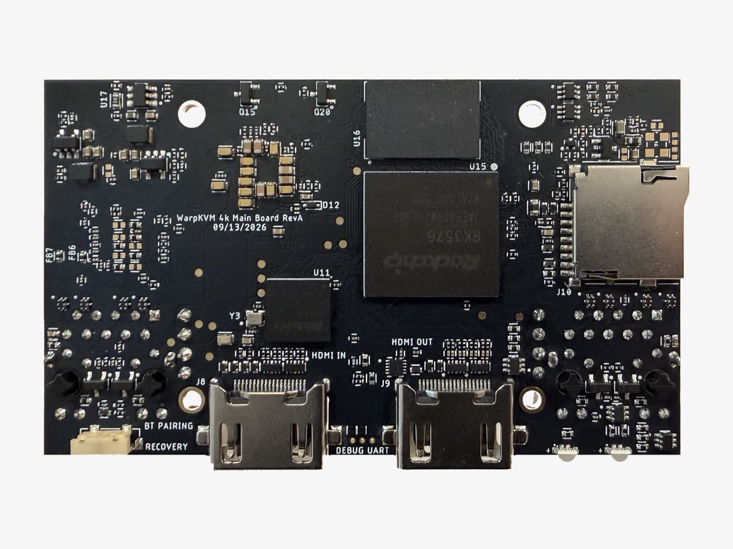
Shown here on our own WarpKVM 01 main board: an RK3576 with an RK628H HDMI bridge, LPDDR4X, an RK806S-5 PMIC and a three-port Ethernet switch, on eight layers. Client boards get the same set.
- 01
Architecture
Chip selection and a block diagram, with a cost and risk view, before any schematic.
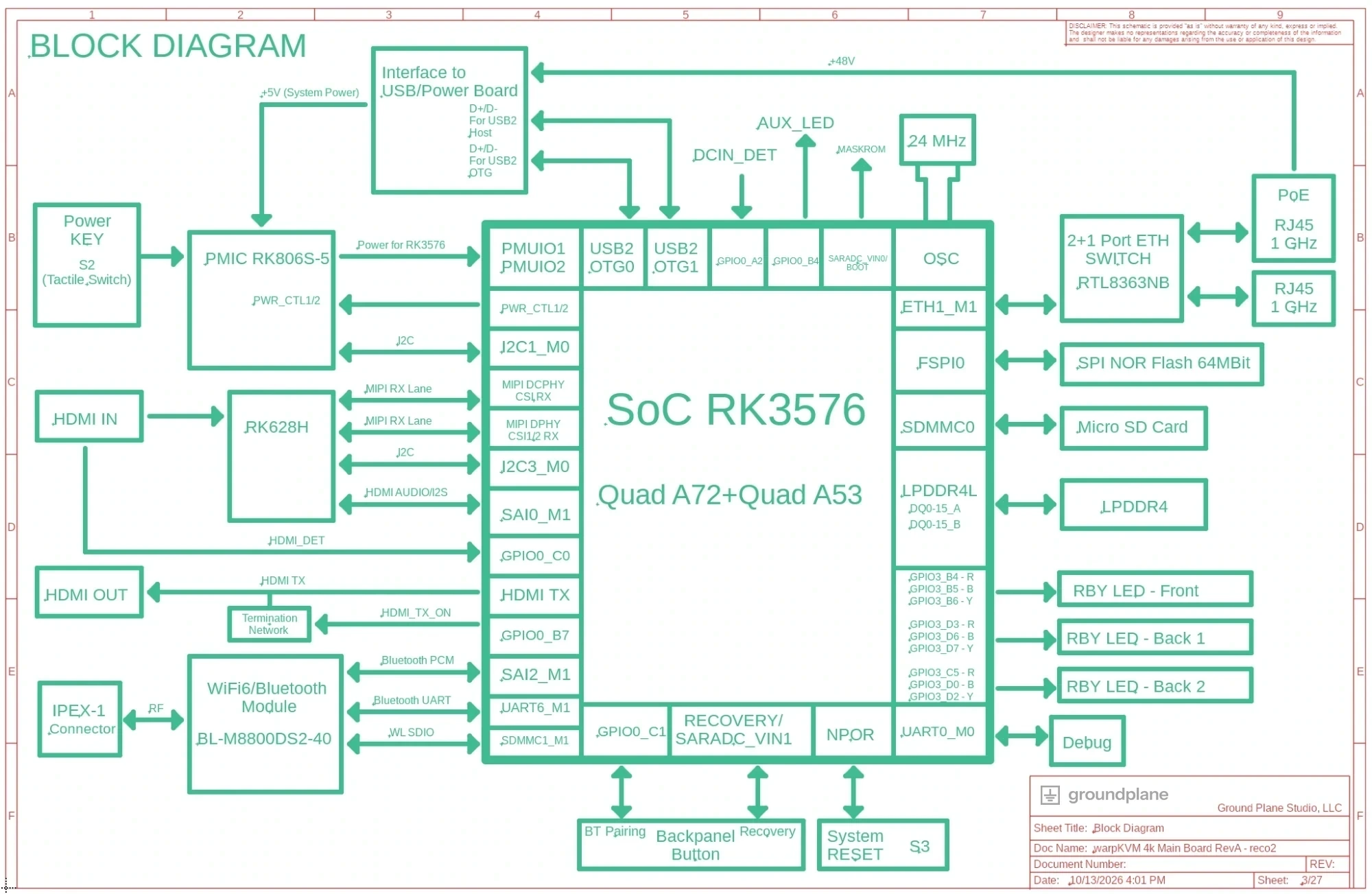
Fig. 2 Block diagram, sheet 3 of 27. - 02
Schematic
Power tree, LPDDR and high-speed I/O, with the alternate functions of every GPIO written beside its pin.
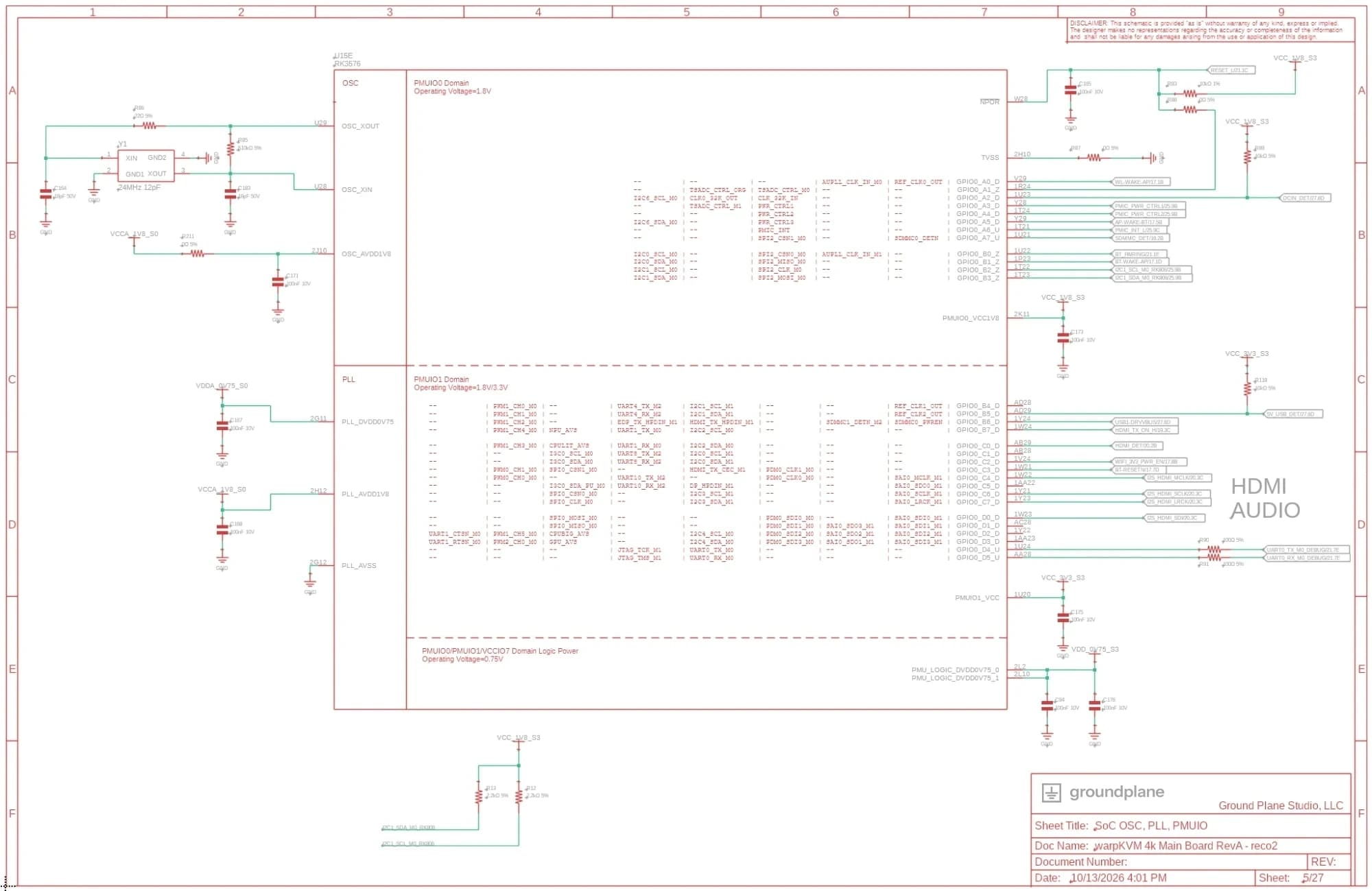
Fig. 3 RK3576 oscillator, PLL and PMU I/O, sheet 5 of 27. - 03
Layout
DDR and high-speed routing, released as Gerbers. WarpKVM 01 is eight layers.
Each copper layer from the fab Gerbers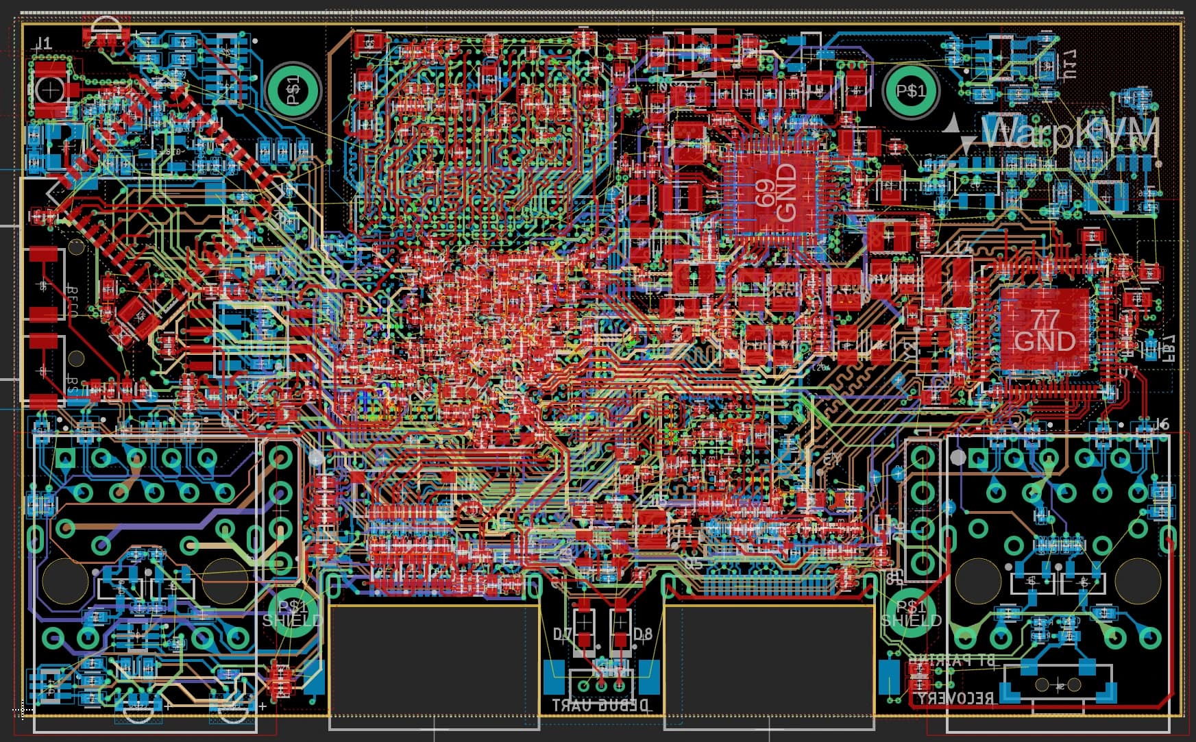
Fig. 4 Layout, all eight layers overlaid. - 04
3D model
The assembled board, connectors and all, for the enclosure and the mechanical fit.
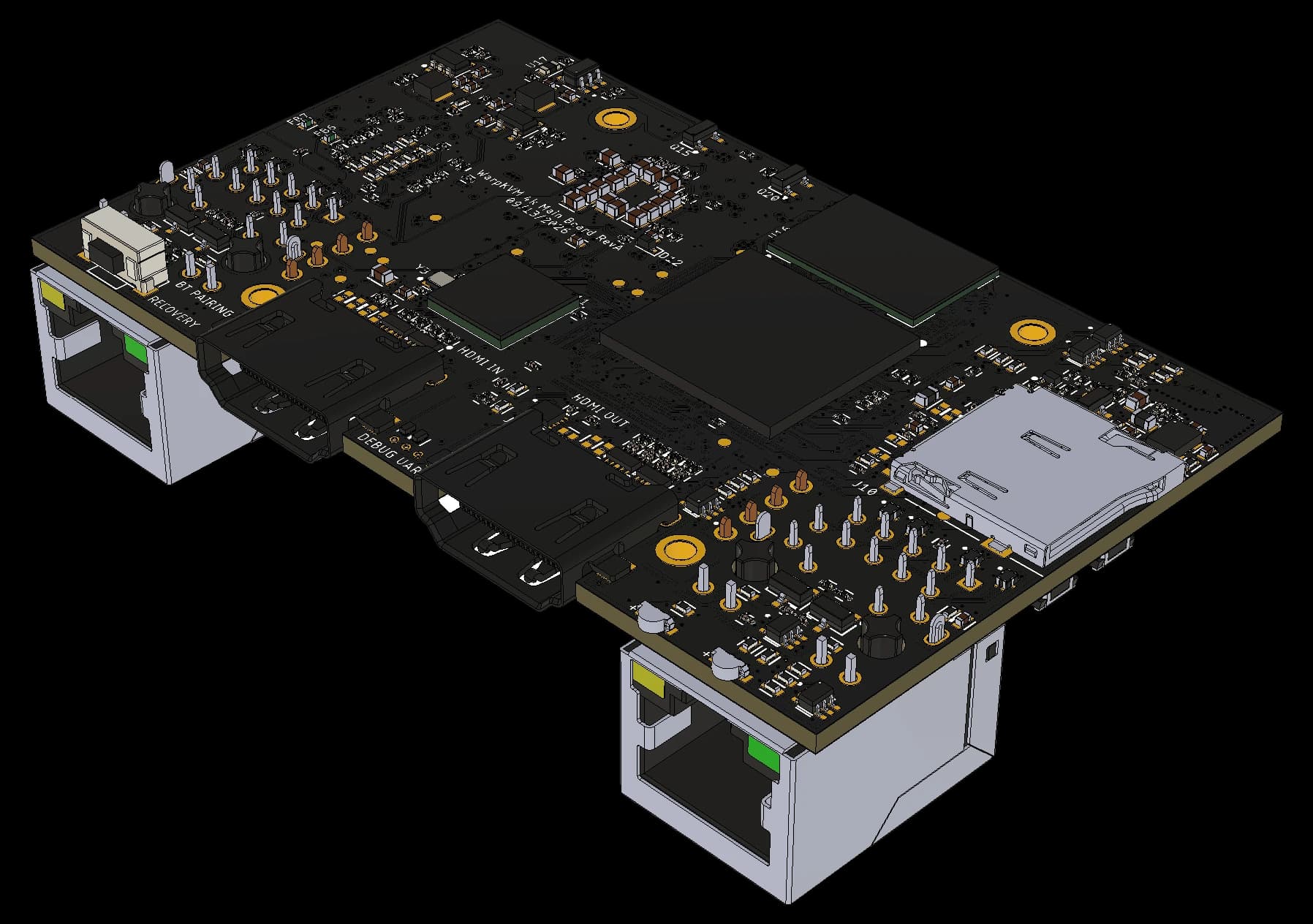
Fig. 5 RK3576 side. 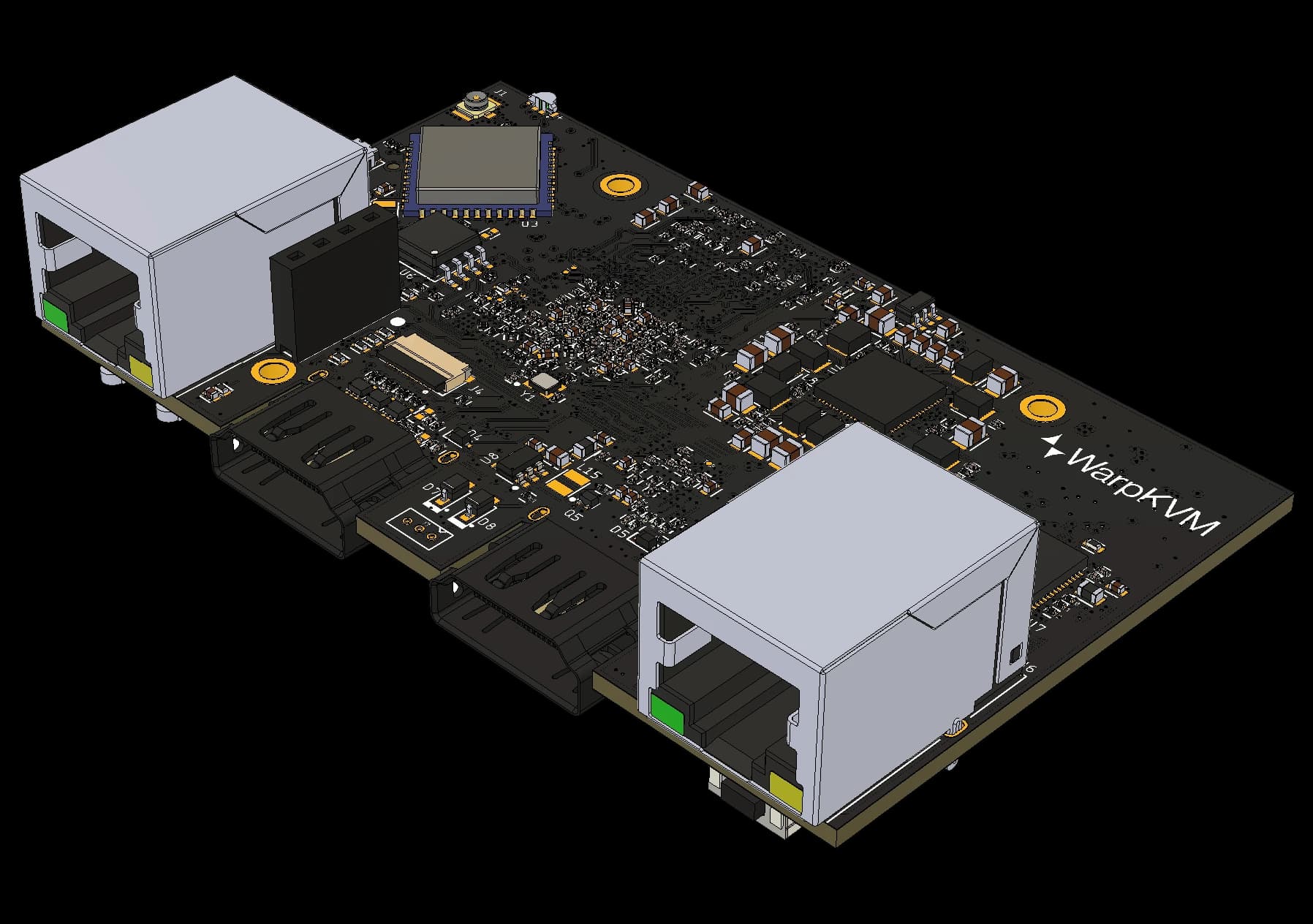
Fig. 6 Wi-Fi side, same angle. - 05
Prototyping
Prototype boards built and brought up on our own bench, with the rest of the system around them. WarpKVM 01 runs with a separate power board, which went from rev A to rev B here.
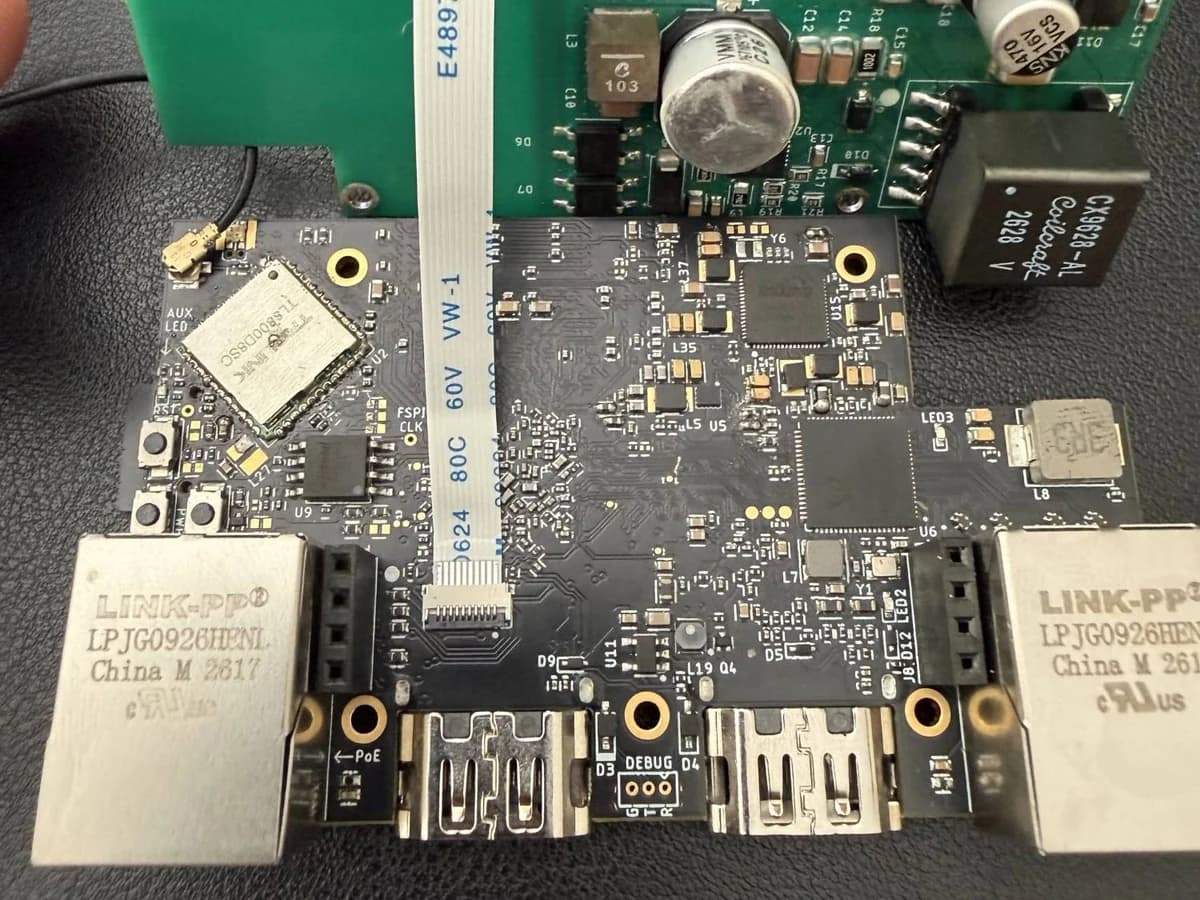
Fig. 7 Main board with power board rev A. 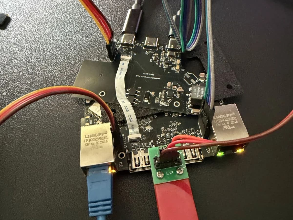
Fig. 8 On the bench: power board rev B, Ethernet up, debug adapter on. - 06
Bring-up and BSP
Power, boot and DDR on our bench, then a device tree, a kernel config and a build that produces bootable media from source. A board that has not booted is not finished.
Fig. 9 DIY WarpKVM (RV1126B), cold boot on the serial console: login prompt at 16.9 s. - 07
Production files
The release a fab and an assembler build from: Gerbers for every layer, drill, pick-and-place for both sides, and a BOM with manufacturer part numbers and JLCPCB codes, flagged where a substitute is fine. Plus a STEP model of the assembled board, the test procedure and programmed media.
warpKVM 4k Main Board RevA, reco2, released 2026-10-13
- GerberFiles/
- copper_l1 to copper_l8, Soldermask_Top/Bot, Paste_Top/Bot, Legend_Top/Bot, Profile_NP, gerber_job.gbrjob16 files
- DrillFiles/
- drill_1_64.xln
- Assembly/
- PnP front, PnP back, BOM403 + 298 placements
- 3D/
- Assembled board, STEPfor the enclosure and mechanical fit
The WarpKVM 01 release package.
Before anything goes to the fab
Every board, ours or yours. A board that fails one of these does not get ordered.
How long it takes
Typical ranges to a first board that boots. Fab time is set by the fab, and a respin adds about 4 to 6 weeks.
| Phase | SoM carrier | Chip-down SoC |
|---|---|---|
| Schematic and layout | 3 to 5 weeks | 6 to 10 weeks |
| Prototype fab and assembly | 2 to 3 weeks | 3 to 4 weeks |
| Bring-up and BSP | 2 to 3 weeks | 4 to 8 weeks |
| First board booting Linux | About 2 months | About 3 to 5 months |
You own it. Respins are on us.
You own the design. Native source files, Gerbers, BOM, pick-and-place, the BSP source and everything else we make for the project are yours, and an NDA is fine before you send anything.
The project price covers the design and the prototype boards, fab and assembly included. If a revision fails because of something in our design, we fix it and build the next one at no charge, as many times as it takes.
A change to the requirements is new work, and we quote it before starting.
Andrew Douglass
Founder, lead designerElectrical design and integration for a decade, including SpaceX launch vehicle and payload integration.
Jamie Alegre
PCB designerCustom layout, high-speed digital design and manufacturing-ready schematics, with design for manufacture on every board.
We write the board firmware and bring in firmware partners when a project needs more hands. For industrial design and anything else outside the board, we work with senior engineers we have shipped with before.
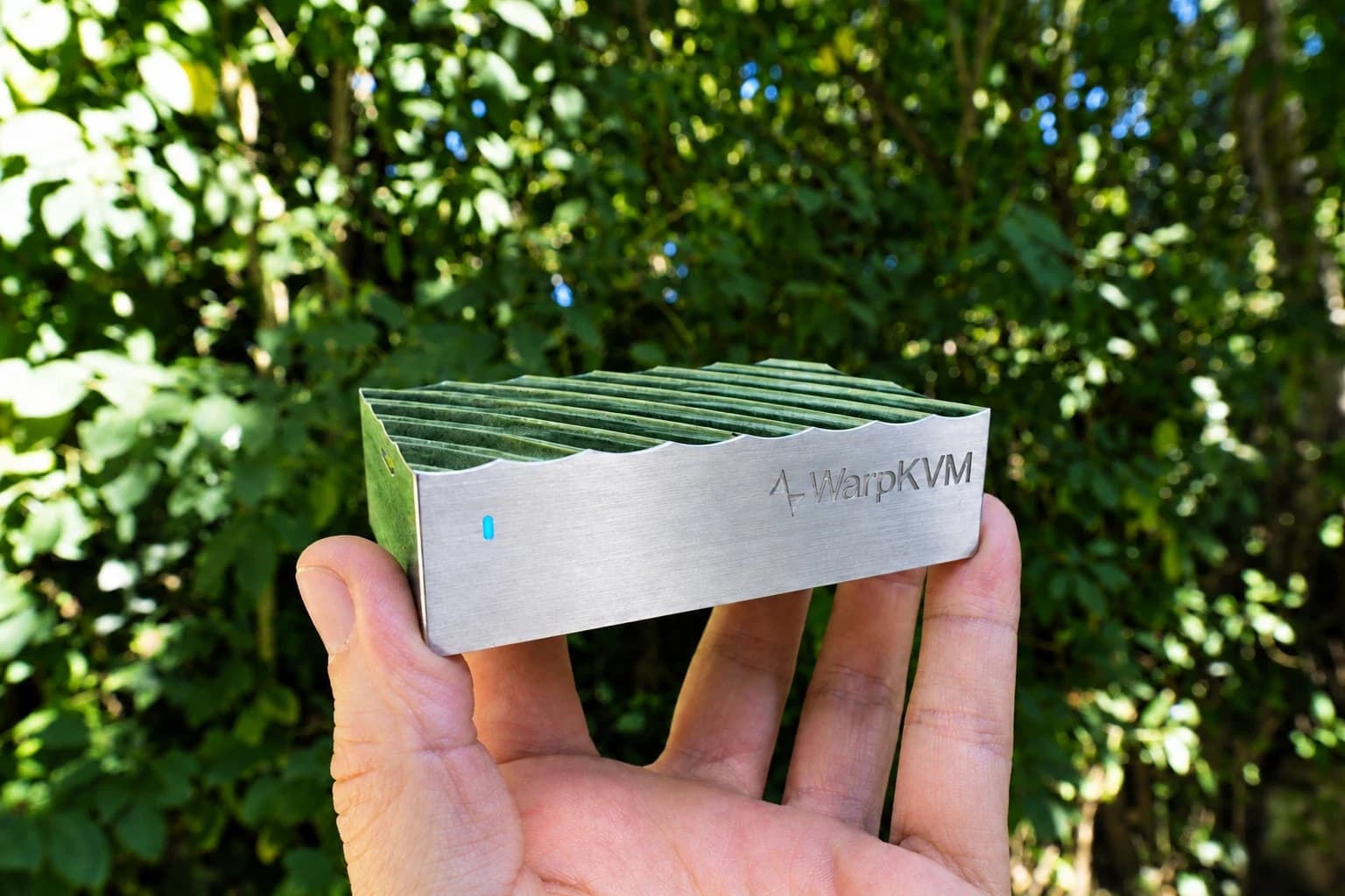
WarpKVM
Our own IP KVM: an eight-layer RK3576 main board with an RK628H HDMI bridge, a Rust streaming daemon, and a light-sensor rig that times the video latency every change adds. Measured at 26.5 ms added at 1080p60 and 35.7 ms at 4K60.

Cloud Gaming Infrastructure
High-density gaming servers, out-of-band management, KVMs, power switching, storage and rack infrastructure for a cloud gaming operator.
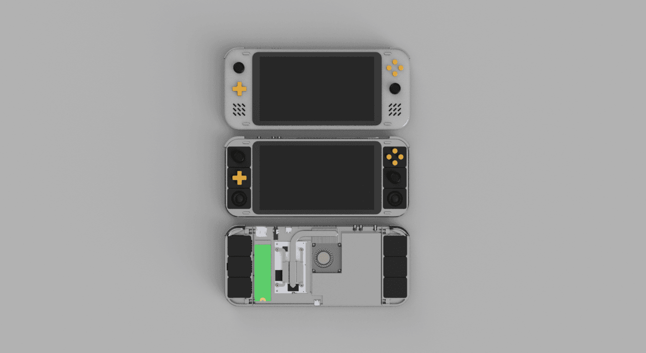
Modular Handheld Controller
A fully modular handheld game console. Swappable input modules, swappable front and back plates, swappable SoC and storage, all on a common backplane bus. Our own product, in active development. Open source at launch.
Frequently asked questions
Rockchip RV1106, RV1126, RV1126B, RK3566, RK3568, RK3576 and RK3588, and Allwinner A527/T527 and T507, each on a board we designed and brought up.
Both. A SoM carrier is faster and lower risk for low volume; chip-down usually wins on unit cost and size once volume justifies the DDR and power work. We will tell you which fits your numbers.
Bring-up, device tree, kernel and BSP, yes, and firmware for companion microcontrollers. Application software is scoped separately.
Usually. Send the files, the boot log and what it does. Power sequencing, DDR training and boot media are the common causes.
A fixed project price that covers design, the prototype boards and bring-up, with respins for our own errors included. It is paid in three parts: 30% at project start, 30% when the prototype boards are ordered and 40% on completion. Production runs are quoted separately.
Yes, for the boards we design. We write the board firmware and software, with firmware partners when a project needs more hands; wire harnesses are built in house to IPC/WHMA-A-620 by certified staff, and enclosure and industrial design go to senior partners we have shipped with.
No. Rockchip and Allwinner SoCs, and carrier boards for the Raspberry Pi CM4 and CM5 and other commercial SoMs, all on the same process. We are open to other chips and other kinds of board too: tell us what you are building.
Send us the files.
An engineer reads them, not a sales team. You get a quote back, or a short list of what we still need to price it.
Replies within two working days.
- The SoC or SoM, if you have chosen one
- The interfaces the product needs
- Power budget, thermal limits and enclosure
- What the software team needs from the BSP
- Target volume and timeline