The DIY WarpKVM runs on the RV1126B, under our RK628H carrier board. Case study: WarpKVM
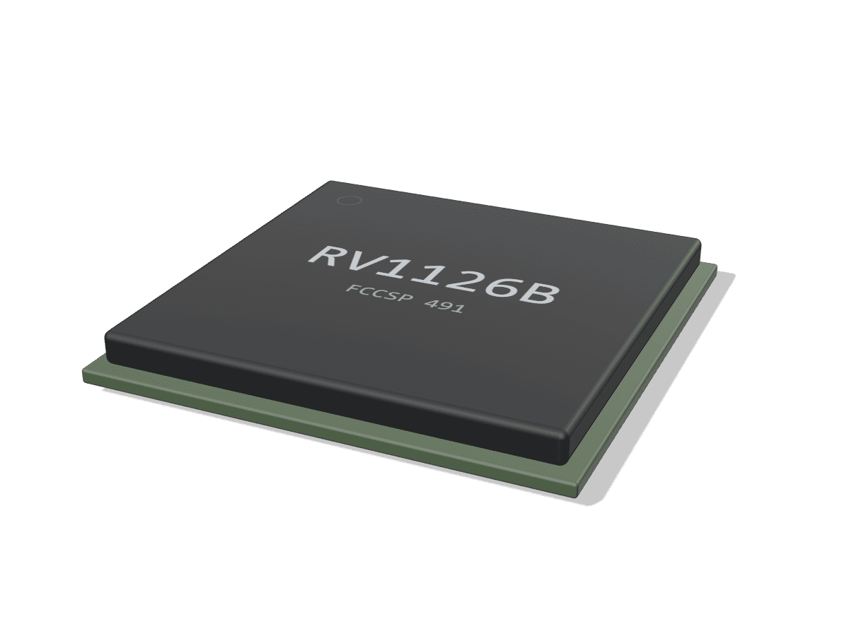
RV1126B
A 64-bit camera SoC for multi-sensor AI vision: quad Cortex-A53, 3 TOPS NPU, 12MP ISP and 4K H.265, with no PCIe, no 3D GPU and a 4 GB RAM ceiling.
- CPU
- 4x Cortex-A53
- GPU
- None (2D RGA only)
- NPU
- 3 TOPS INT8
- Video
- Enc 12M@30, dec 4K30 (H.265/H.264)
- PCIe
- None
What the RV1126B is for
Right for
- AI IP cameras and smart vision nodes: 12MP@30 ISP, 8MP AI-ISP and H.265/H.264 encode up to 12M@30 on one chip
- Multi-camera designs: two 4-lane MIPI CSI ports (splittable to four 2-lane) plus a 16-bit DVP, up to four sensors at once
- Upgrading an existing RV1126 board: the RV1126B-P is pin-to-pin with RV1126 and moves it to 64-bit Cortex-A53 and a 3 TOPS NPU
- Stitched or fisheye cameras: hardware fisheye correction (about 4K30) and the AVSP stitching block
- Small Linux gateways that need USB 3.0, gigabit RGMII, an on-chip 10/100 PHY and two CAN ports
Wrong for
- Designs needing PCIe, SATA or HDMI: none of them exist on the chip
- GPU-rendered UIs: there is no 3D GPU, only the 2D RGA engine
- More than 4 GB of RAM: the DDR interface is 32-bit with 4 GB total address space
- More than one display, or output above 1920x1080@60
- Products that must run a mainline kernel today: as of Linux 7.3-rc7 there is no RV1126B SoC devicetree or pinctrl in mainline
Cost and constraints
- Software is the Rockchip IPC SDK on Linux 6.1 and U-Boot 2017.09; the SDK is fetched from Rockchip gerrit with an account, though board vendors (Luckfox, Boardcon, Forlinx) ship their own SDK packages
- The 3 TOPS figure carries a "Sparsity" footnote in the datasheet; dense throughput is not stated
- The full RV1126B is a 491-ball 14x14 mm FCCSP with 0.25 mm balls on mixed 0.42/0.5/0.65 mm pitch; the RV1126B-P is 409 balls at a uniform 0.65 mm pitch but drops USB 3.0, the audio codec and the Ethernet PHY
- No public TRM, hardware design guide or Rockchip EVB schematic was found; the public design references are vendor manuals and the Luckfox Aura schematic
- No public bare-chip pricing or distributor listing was found; volume pricing goes through Rockchip agents or module vendors
Inside the RV1126B
Drawn by Groundplane from the datasheet rev 1.1. Not Rockchip artwork.
- DDR3/3L/4, LPDDR3/4/4X x32
- eMMC 4.51 HS200
- SD 3.0
- FSPI quad, 2 CS
- 4x Cortex-A53, 512 KB L2
- HPMCU, 16 KB cache
- LPMCU, always-on domain
- 3 TOPS INT8 (sparse)
- INT4, INT8, INT16, FP16
- ISP 12M@30fps
- AI-ISP 8M@30fps
- H.265/H.264 enc 12M@30
- H.265/H.264 dec 4K@30
- JPEG enc and dec
- RGA 2D, VPSS, FEC, AVSP
- 32-bit DDR controller, 4 GB
- 64 KB SRAM, 8 KB PMU SRAM
- VOP, 1920x1080@60
- VICAP, 4 MIPI groups
- DVP capture
- 3x SAI, LP SAI, PDM 8ch
- 2x audio ADC, DSM DAC
- Crypto: AES, SM4, RSA, SM2
- Secure OTP 8 Kbit, TrustZone
- 4 PLLs, 24 MHz osc
- RTC, POR, watchdogs
- TS-ADC 2ch, 3x SARADC
- USB 3.0 DRD
- USB 2.0 host
- GMAC RGMII or RMII
- 10/100 Ethernet PHY
- SDIO 3.0
- 2x MIPI CSI 4-lane or 4x 2-lane
- DVP BT.601/656/1120
- MIPI DSI 4-lane
- RGB/MCU 24-bit
- 2x CAN, 8x UART, 6x I2C
- 2x SPI, 28 PWM ch, DSMC
Read from the documents
Each value names the document it was read from.
| CPU | 4x Cortex-A53 (Armv8-A), 32 KB I + 32 KB D L1 per core, 512 KB shared L2, NEON and FPU; cores 3 and 4 on separate power domains | Datasheet Rev 1.1, 1.2.1 |
|---|---|---|
| CPU clock | Up to 1.6 GHz (RV1126B), 1.3 GHz (RV1126BJ); the Rockchip datasheet does not state a maximum clock | Other V1.2 |
| Companion MCUs | HPMCU with 16 KB cache; LPMCU in the always-on PMU domain for low-power video (AOV) and audio (AOA) wake | Datasheet Rev 1.1, 1.2.3 to 1.2.5 |
| GPU | No 3D GPU. 2D RGA: 8192x8192 source, 4096x4096 destination, scale 1/16 to 16, rotate, blend | Datasheet Rev 1.1, 1.2.8 |
| NPU | 3 TOPS INT8 (footnoted "Sparsity"); INT4, INT8, INT16 and FP16; own voltage domain with DVFS | Datasheet Rev 1.1, 1.2.7 |
| Video decode | H.265 Main L5.0 and H.264 Main L5.1 up to 3840x2160@30; JPEG baseline decode | Datasheet Rev 1.1, 1.2.6 |
| Video encode | H.265 Main L5.0 High tier, H.264 High L5.0, JPEG; up to 12M@30fps, up to 200 Mbps; parallel H.26x plus JPEG | Datasheet Rev 1.1, 1.2.6 |
| ISP | 12M@30fps ISP (HDR 2-frame merge, 3DNR, PDAF, RGB-IR); 8M@30fps AI-ISP; up to 2 sensors share the ISP; fisheye correction about 3840x2160@30 | Datasheet Rev 1.1, 1.2.12 |
| Camera | 2x MIPI D-PHY v1.2 (CSI, LVDS or SubLVDS), 4 lanes at 2.5 Gbps/lane each, each splittable to 2x 2-lane; DVP 8 to 16-bit up to 150 MHz, BT.601/656/1120; up to four sensors simultaneously | Datasheet Rev 1.1, 1.1, 1.2.11 |
| Memory | 32-bit DDR3, DDR3L, DDR4, LPDDR3, LPDDR4, LPDDR4X; 2 ranks; 4 GB total address space | Datasheet Rev 1.1, 1.2.2 |
| Storage | eMMC 4.51 with HS200 (no command queue), SD 3.0 / MMC 4.51, FSPI 1/2/4-bit with 2 chip selects | Datasheet Rev 1.1, 1.2.2 |
| Display | One VOP up to 1920x1080@60: 4-lane MIPI DSI at 1.5 Gbps/lane, RGB/MCU up to 24-bit, BT.656/BT.1120 | Datasheet Rev 1.1, 1.2.9, 1.2.10 |
| PCIe | None | Datasheet Rev 1.1, 1.2.16 |
| USB | 1x USB 3.0 DRD (xHCI), 1x USB 2.0 host (EHCI/OHCI) | Datasheet Rev 1.1, 1.2.16 |
| Ethernet | 1x GMAC: RGMII 10/100/1000 or RMII 10/100, or the integrated 10/100 PHY; TSO/USO offload, IEEE 1588 timestamps | Datasheet Rev 1.1, 1.2.16 |
| Audio | 3x SAI (I2S/PCM/TDM) plus a low-power SAI, 8-channel PDM, 2 integrated audio ADCs, 2-channel digital DAC (DSM), dual ASRC | Datasheet Rev 1.1, 1.2.15 |
| Other I/O | 2x CAN (ISO 11898-1:2003; Rev 1.1 said CAN FD), 8x UART (RS485 on UART1 to 7), 6x I2C, 2x SPI, 4 PWM blocks with 28 channels, 3x 8-channel 13-bit SARADC, SDIO 3.0, DSMC parallel bus | Datasheet Rev 1.4, 1.2.16, 1.2.17 |
| Security | Crypto engine (AES, SM4, SHA-1/256, SM3, RSA to 4096, ECC to 256, SM2), key ladder, 8 Kbit OTP (6.5 Kbit secure), TrustZone, secure boot and debug | Datasheet Rev 1.1, 1.2.3, 1.2.17 |
| Boot | Boot ROM boots from SPI flash, eMMC or SD; code download over USB 2.0 or UART | Datasheet Rev 1.1, 1.2.2 |
| Package | RV1126B: FCCSP 491, 14x14 mm, 0.25 mm balls, 0.42/0.5/0.65 mm mixed pitch. RV1126B-P: FCCSP 409, 14x14 mm, 0.3 mm balls, 0.65 mm pitch. MSL3, SnAgCu | Datasheet Rev 1.1, 1.2.17, 2.4, 2.5 |
| Thermal | Tj max 125 C; theta-JA 28.2 C/W, theta-JB 6.06 C/W, theta-JC 1.50 C/W (JEDEC 2S2P simulation) | Datasheet Rev 1.1, 4.1, 4.2 |
Variants
| RV1126B | Full-featured version: FCCSP 491, USB 3.0 DRD, integrated audio codec (2 ADCs), integrated 10/100 Ethernet PHY, 24 SARADC inputs, built-in RTC, MIPI CSI as 2x 4-lane or 4x 2-lane. | Other V1.0.0 |
|---|---|---|
| RV1126B-P | Pin-to-pin with the original RV1126 (FCCSP 409, 0.65 mm) so RV1126 boards can take it without a hardware redesign, per Rockchip. Same Cortex-A53 and 3 TOPS NPU, but USB 2.0 only (DRD plus host), no audio ADC, no Ethernet PHY (GMAC only), 6 SARADC inputs, no RTC. Rockchip pairs it with RK809 on its EVB; a separate RV1126 to RV1126B-P compatibility note exists but was not found publicly. | Other V1.0.0 |
| RV1126BJ | Industrial grade, own datasheet (Rev 1.1, 2025-09-30): -40 to 85 C ambient against -20 to 85 C for the RV1126B (datasheet Rev 1.4), same FCCSP 491 package and feature list. Neither datasheet states a CPU clock; Forlinx lists the BJ at up to 1.3 GHz (vs 1.6 GHz). | Datasheet Rev 1.1 |
What to watch when you design with it
Power and PMIC
Rockchip names its reference power solution in the SDK board configs: RK801 on the RV1126B EVB1 V10/V11 and RK809 on the RV1126B-P EVB1 V10/V11. The Luckfox Aura SDK also builds for RK801, and a community schematic uses the RK801-2. RK801 is an I2C PMIC with 4 buck converters, 2 LDOs and 1 switch; its driver landed in mainline Linux 7.0. No public RK801 datasheet was found, so sequencing and rail voltages have to come from a vendor schematic or Rockchip. The SoC has four supply domains (CPU_DVDD, NPU_DVDD, VDD_LOGIC, VDD_PMU) with CPU and NPU each on an isolated DVFS rail. Forlinx specifies a 5 V input with at least 2.5 A to its SoM.
Sources: Other V1.6.0, Datasheet Rev 1.1, PMIC, PMIC Rev 1.1, Other V1.2
DDR
One 32-bit channel, two ranks, 4 GB maximum, with DDR3, DDR3L, DDR4, LPDDR3, LPDDR4 or LPDDR4X. Shipping boards use LPDDR4X (Luckfox Aura), LPDDR4 (Forlinx, Boardcon) and DDR3 (Graperain default). Rockchip publishes its validated DDR part list on its redmine portal, which needs an account. No public RV1126B DDR layout guide was found; vendor SoMs put the DDR on 8-layer (Boardcon, Graperain) or 10-layer (Forlinx) boards.
Sources: Datasheet Rev 1.1, Other V1.6.0, Other V1.2, armdesigner.com, embsom.com
Boot and maskrom
The boot ROM tries SPI flash, eMMC and SD, and accepts code over USB 2.0 or UART. On the Forlinx SoM, pulling SARADC0_IN7_BOOT to ground at power-up enters maskrom, boot order is FSPI, eMMC, TF, USB, and only the USB 3.0 OTG port (USB0) can flash the system. Rockchip EVBs enter maskrom by holding Update and pressing Reset. The debug UART runs at 1,500,000 baud, which rules out CH340 and PL2303 adapters per Luckfox. Keep the debug UART and the OTG port reachable on any custom board.
Sources: Datasheet Rev 1.1, Other V1.2, Other V1.6.0, wiki.luckfox.com
High-speed interfaces
MIPI CSI runs at up to 2.5 Gbps/lane and DSI at 1.5 Gbps/lane. Forlinx routes all USB pairs at 90 ohm differential, notes that USB_OTG_VBUSDET must see VBUS for USB to work, and for the on-chip 10/100 PHY places 110 ohm terminations across FEPHY TX and RX near the SoC, 5.1 ohm series resistors near the transformer and a 1 nF center-tap capacitor. The on-chip PHY and an external RGMII PHY share the single GMAC, so only one Ethernet port works at a time.
Sources: Datasheet Rev 1.1, Other V1.2, armdesigner.com
Thermal
Maximum junction temperature is 125 C. Datasheet Rev 1.1 gives theta-JA 28.2 C/W on a 4-layer JEDEC board, theta-JC 1.50 C/W. Forlinx measured its SoM at 1.51 W with 100% CPU and its dev board at 4.66 W with camera, 7 inch display and video running. Vendor operating ranges: -20 to +85 C (Forlinx RV1126B), -40 to +85 C (RV1126BJ), -20 to +70 C (Boardcon modules).
Sources: Datasheet Rev 1.1, Other V1.2, armdesigner.com
Gotchas
RV1126B-P fits an RV1126 footprint, but software does not carry over: the pinctrl registers differ from RV1126 (stated in the upstream pinctrl patch), the CPU moves from 32-bit to 64-bit, and the NPU needs RKNN-Toolkit2 rather than the legacy toolkit used by RV1126. The RV1126B-P also loses USB 3.0, the audio ADCs and the Ethernet PHY relative to RV1126B.
Sources: Other V1.0.0, lkml.iu.edu, github.com
Layout guides for the RV1126B's interfaces
Public layout guidance for each interface this chip has, from vendors who publish it, plus our calculators.
LPDDR4
Point-to-point routing; TI notes that on-die termination on both ends means no board termination is needed. Byte lanes length-matched to their strobe and command/address matched to the clock, all over a solid reference plane. Impedance targets differ by vendor: TI AM62x and ADI EE-480 use 40 ohm single-ended and 80 ohm differential, Synaptics SL1680 uses 50 and 85 ohm, AMD Versal 45 and 82 ohm. Use the SoC vendor's own target and simulate.
- AM62x, AM62Lx DDR Board Design and Layout GuidelinesTexas Instruments, SPRAD06, C, 2025
- AM62Ax, AM62Px, AM62Dx LPDDR4 Board Design and Layout GuidelinesTexas Instruments, SPRAD66, B, 2024
- ADSP-2184x/ADSP-SC84x LPDDR4 Board Design GuidelinesAnalog Devices, EE-480, 1, 2026
- SL1680 General PCB Design and LPDDR4 & LPDDR4(x) Interface Layout GuidelinesSynaptics, PN 506-001390-01, E
- DDR length matching calculatorGroundplane calculator
LPDDR4X
Same topology and matching discipline as LPDDR4, with a lower I/O voltage, so routing rules are usually published for both together. Synaptics SL1680 gives 50 ohm single-ended and 85 ohm differential for LPDDR4 and LPDDR4X; AMD Versal gives 45 and 82 ohm. Check the SoC vendor target before fixing the stackup.
- SL1680 General PCB Design and LPDDR4 & LPDDR4(x) Interface Layout GuidelinesSynaptics, PN 506-001390-01, E
- SL1640 General PCB Design and DDR4 & LPDDR4(x) Interface Layout GuidelinesSynaptics, PN 506-001529-01, D
- Versal Adaptive SoC PCB Design User Guide: PCB Routing Guidelines for LPDDR4/4x InterfacesAMD, UG863, 1.12, 2026
- DDR length matching calculatorGroundplane calculator
DDR4
DDR4 uses pseudo open-drain data signaling and needs a VPP supply, with command/address routed fly-by or as a balanced tree depending on device count. TI AM62x uses 40 ohm single-ended and 80 ohm differential; AMD Versal uses 50 and 90 ohm, relaxed under the BGA. Match data to strobe per byte and command/address to clock.
- AM62x, AM62Lx DDR Board Design and Layout GuidelinesTexas Instruments, SPRAD06, C, 2025
- Versal Adaptive SoC PCB Design User Guide: PCB Routing Guidelines for DDR4 InterfacesAMD, UG863, 1.12, 2026
- SL1640 General PCB Design and DDR4 & LPDDR4(x) Interface Layout GuidelinesSynaptics, PN 506-001529-01, D
- PCB Design Guidelines (HSSI, EMIF, MIPI, True Differential, PDN) User Guide: Agilex 5 FPGAs and SoCsAltera, 821801, 2026
- DDR length matching calculatorGroundplane calculator
- Via current calculatorGroundplane calculator
DDR3 / DDR3L
Fly-by command/address with termination at the end of the chain, point-to-point data lanes matched to their strobe, and a clean VREF. ST recommends 55 ohm single-ended and 100 ohm differential for DDR3 and DDR3L on STM32MP1 boards, and shows that a 4-layer board is possible with strict layer allocation.
- STM32MP1 Series DDR memory routing guidelinesSTMicroelectronics, AN5122, 3, 2019
- DDR3 Design Requirements for KeyStone DevicesTexas Instruments, SPRABI1, D, 2022
- SL2610 General PCB Design and DDR3L/DDR4 & LPDDR4(x) Interface Layout GuidelinesSynaptics, PN 506-001629-01, A, 2025
- DDR length matching calculatorGroundplane calculator
LPDDR3
Point-to-point and normally unterminated, with command/address matched to the clock and each byte matched to its strobe. ST gives the same targets for LPDDR3 as for DDR3: 55 ohm single-ended and 100 ohm differential. Few current public guides cover LPDDR3, so treat the SoC vendor's reference layout as the stronger source.
- STM32MP1 Series DDR memory routing guidelinesSTMicroelectronics, AN5122, 3, 2019
- DDR length matching calculatorGroundplane calculator
eMMC
A single-ended bus: CLK, CMD, DAT0 to DAT7 and, for HS400, the data strobe. TI and Synaptics both route it at 50 ohm single-ended, match the group, and keep stubs short; Synaptics places a 22 or 33 ohm series resistor on CLK and STRB. At HS400 TI also checks the eMMC I/O supply impedance, not just the traces.
- AM62Px eMMC HS400 Board Design and Simulation GuidelinesTexas Instruments, SPRADP5, A, 2026
- Astra Machina Foundation Series eMMC ConfigurationSynaptics, PN 506-001594-01, D
- i.MX28 Layout and Design GuidelinesNXP (Freescale), AN4215, 0, 2010
SD card / SDIO
Single-ended CLK, CMD and four data lines over a solid ground plane, at constant trace width and matched length. NXP asks for clock-to-neighbor spacing greater than twice the trace height above the plane and 1.5 times for data and CMD, with 45 degree bends. UHS modes switch the I/O to 1.8 V, so a level translator often sits next to the socket.
- NVT4557/NVT4558/NVT4858 voltage-level translator layout guidelineNXP, AN13158, 1.1, 2022
- i.MX28 Layout and Design GuidelinesNXP (Freescale), AN4215, 0, 2010
- SD Physical Layer Simplified SpecificationSD Association, 9.10, 2023
PCIe
AC-coupled differential lanes routed with no stubs, minimal vias and back-drilled or blind vias where speed demands, with lane-to-lane skew handled by the receiver. Targets differ by guide: TI Jacinto 7 uses 85 ohm differential for lanes and 100 ohm for the reference clock, while TI's earlier SoC guide tabulates 100 ohm and, for some devices, 95 ohm. Match the target to your connector and stackup.
- Jacinto7 AM6x, TDA4x, and DRA8x High-Speed Interface Design GuidelinesTexas Instruments, SPRACP4, A, 2024
- High-Speed Interface Layout GuidelinesTexas Instruments, SPRAAR7, J, 2023
USB 3.x
SuperSpeed TX and RX pairs are routed at 90 ohm differential in all three TI guides (SPRAAR7 lists 95 ohm for some devices), with AC coupling capacitors on TX, symmetric pad and via placement, and matched via counts within each pair. Keep the pairs away from the USB 2.0 pair and other aggressors, and place ESD at the connector.
- High-Speed Layout Guidelines for Signal Conditioners and USB HubsTexas Instruments, SLLA414, A, 2026
- Jacinto7 AM6x, TDA4x, and DRA8x High-Speed Interface Design GuidelinesTexas Instruments, SPRACP4, A, 2024
- High-Speed Interface Layout GuidelinesTexas Instruments, SPRAAR7, J, 2023
USB 2.0
One D+/D- pair at 90 ohm differential, routed in parallel for its whole length with minimal deviations at the connector and package. NXP keeps clocks and periodic signals at least 50 mils away and other signals at least 20 mils away from the pair.
- High-Speed Layout Guidelines for Signal Conditioners and USB HubsTexas Instruments, SLLA414, A, 2026
- High-Speed Interface Layout GuidelinesTexas Instruments, SPRAAR7, J, 2023
- i.MX28 Layout and Design GuidelinesNXP (Freescale), AN4215, 0, 2010
MIPI DSI
MIPI D-PHY clock and data lanes are routed as 100 ohm differential pairs over a solid reference; TI Jacinto 7 allows no stubs, 2 vias per trace and 40 ps lane-to-lane skew. Connectors and flex cables to the panel are usually the largest discontinuity, so keep the board segment short and clean.
- Jacinto7 AM6x, TDA4x, and DRA8x High-Speed Interface Design GuidelinesTexas Instruments, SPRACP4, A, 2024
- PCB Design Guidelines (HSSI, EMIF, MIPI, True Differential, PDN) User Guide: Agilex 5 FPGAs and SoCsAltera, 821801, 2026
MIPI CSI-2
Same D-PHY rules as DSI: 100 ohm differential lanes in both TI guides, with lane-to-lane skew bounded (40 ps in TI Jacinto 7). Size the lane count and lane rate from the sensor's output format before routing.
- Jacinto7 AM6x, TDA4x, and DRA8x High-Speed Interface Design GuidelinesTexas Instruments, SPRACP4, A, 2024
- High-Speed Interface Layout GuidelinesTexas Instruments, SPRAAR7, J, 2023
- PCB Design Guidelines (HSSI, EMIF, MIPI, True Differential, PDN) User Guide: Agilex 5 FPGAs and SoCsAltera, 821801, 2026
- MIPI CSI-2 bandwidth calculatorGroundplane calculator
LVDS
Tightly coupled differential pairs terminated at the receiver in 100 ohm, with TI's EMI guide asking for 100 ohm differential traces within 5 percent. Keep pairs matched and away from other aggressors, and avoid stubs and reference plane gaps along the route to the panel connector.
- LVDS Owner's Manual: Including High-Speed CML and Signal ConditioningTexas Instruments, SNLA187, 4th edition, 2008
- High-Speed Layout Guidelines for Reducing EMI for LVDS SerDes DesignsTexas Instruments, SNLA302, 2018
- LVDS SerDes Gen I PCB and Interconnect Design-In GuidelinesTexas Instruments, SNLA008, A, 2018
Ethernet (RGMII / RMII)
TI routes MAC-to-PHY (MII family) traces at 50 ohm single-ended, under 6 inches, matched within 20 mils for gigabit, and the PHY-side MDI pairs at 100 ohm differential. RGMII also needs a 1.5 to 2.0 ns clock-to-data delay, added on the board or inside the MAC or PHY (RGMII-ID); decide which before layout so it is not applied twice.
- Ethernet PHY PCB Design Layout ChecklistTexas Instruments, SNLA387, 2021
- PCB Design Guideline for RGMII InterfaceRenesas, R01AN6272EJ0141, 1.41, 2026
- i.MX28 Layout and Design GuidelinesNXP (Freescale), AN4215, 0, 2010
Board-level design guides
Impedance and timing, power, thermal and ESD guidance that applies to any board around this chip.
Impedance and timing
Every high-speed interface on the board comes down to the same two numbers: the trace impedance your stackup actually gives, and the delay each trace adds. Set the stackup with your fab first, then route to its impedance table and match lengths in time, not millimeters, where the layers differ.
- High-Speed Interface Layout GuidelinesTexas Instruments, SPRAAR7, J, 2023
- PCB impedance calculatorGroundplane calculator
- PCB propagation delay calculatorGroundplane calculator
Power delivery
For each switching regulator, place and route the input capacitor first, keep the switching current loop small, and keep the switch node short. Give the SoC rails solid planes and decoupling at the balls, and size current-carrying copper and vias for the real load.
- Five steps to a great PCB layout for a step-down converterTexas Instruments, SLYT614, 2015
- AN-1149 Layout Guidelines for Switching Power SuppliesTexas Instruments, SNVA021, C, 2013
- AN-1229 SIMPLE SWITCHER PCB Layout GuidelinesTexas Instruments, SNVA054, C, 2013
- Buck converter calculatorGroundplane calculator
- LDO power dissipation calculatorGroundplane calculator
- PCB trace width calculatorGroundplane calculator
- Via current calculatorGroundplane calculator
Thermal
Theta-JA is measured on a JEDEC test board that carries most of the heat, so it does not transfer directly to a product board; use it to compare packages and use the psi metrics for estimates. Thermal vias under the package, copper area and copper thickness move the most heat into the board.
- Semiconductor and IC Package Thermal MetricsTexas Instruments, SPRA953, D, 2024
- AN-2020 Thermal Design By Insight, Not HindsightTexas Instruments, SNVA419, C, 2013
- Heatsink thermal resistance calculatorGroundplane calculator
- LDO power dissipation calculatorGroundplane calculator
ESD protection
Place the TVS as close to the connector as design rules allow, route from the connector to the TVS with no stub, and keep the protected IC further from the TVS than the TVS is from the connector. Choose parts by clamping performance and by capacitance low enough for the interface speed.
- ESD Protection Layout GuideTexas Instruments, SLVA680, A, 2022
- Reading and Understanding an ESD Protection Data SheetTexas Instruments, SLLA305, A
- TPD12S016 PCB Layout Guidelines for HDMI ESDTexas Instruments, SLLA324, 2012
- PCB conductor spacing calculator (IPC-2221)Groundplane calculator
Rockchip's hardware design guide
Rockchip's hardware design guide, EVB reference schematics and DDR templates come from Rockchip or an authorized agent, usually under NDA, or through your SoM vendor. We do not link copies circulating elsewhere. The vendor schematics and open designs on the Boards tab are real, shipped layouts on the RV1126B and the best public reference.
BSP, mainline and toolkits
| Area | Status | Links |
|---|---|---|
| Vendor BSP kernel | Rockchip RV1126B Linux IPC SDK on Linux 6.1 (V1.0.0 released 2025-06-20; Quick Start V1.6.0 dated 2025-09-30). Vendor builds: Boardcon and Forlinx ship 6.1.141, Boardcon IPC fastboot images 6.1.157. Rockchip distributes the SDK through gerrit with an account; Luckfox publishes its own SDK tarball for the Aura.Checked 2026-10-13 | |
| Mainline Linux | Partial, no bootable board yet. Clock and reset controller (clk-rv1126b) and power domains landed in 6.19; RK801 PMIC MFD and regulator support in 7.0. RV1126B pinctrl was posted (v4, December 2025) but is not in mainline as of 7.3-rc7, and there is no RV1126B SoC dtsi or board devicetree. No NPU, VPU, ISP or display support upstream.Checked 2026-10-13 | |
| U-Boot | Vendor U-Boot v2017.09 in the Rockchip SDK. Mainline U-Boot has only the RV1126B clock and power dt-binding headers synced from Linux, no SoC or board support.Checked 2026-10-13 | |
| NPU toolkit | RKNN-Toolkit2 added RV1126B in v2.3.2 (2025-04-09); the README changelog for v2.5.0 adds a mini runtime and MatMul API for RV1126B. Use target_platform rv1126b. RKNN-LLM lists the RV1126B series as supported.Checked 2026-10-13 | |
| Video (MPP) and 2D (RGA) | Rockchip MPP and librga both reference RV1126B in their public source and changelogs. The IPC SDK media stack (Rockit runtime, ISP35 tuning) ships inside the vendor SDK; Rockchip guides for both are mirrored in the Luckfox docs repository.Checked 2026-10-13 | |
| Distributions | Buildroot from the Rockchip SDK; Debian 13 images for the Luckfox Aura; Debian 12 and Buildroot from Boardcon. No Armbian or Ubuntu support was found.Checked 2026-10-13 | |
| Community | Luckfox forums and wiki carry most public RV1126B discussion; CNX Software has covered each module launch.Checked 2026-10-13 |
RV1126B on GitHub
Repositories for this chip: vendor code, mainline work, toolkits, distributions and open hardware.
- Vendor BSPLuckfoxTECH/luckfox-aura-docsLuckfox documentation and hardware resources for the RV1126B based Luckfox Aura, including the public RV1126B datasheet and BSP guides. Last commit 2026-07.
- Kernelrockchip-linux/kernelRockchip BSP kernel; RV1126B device trees are on develop-6.1, the SDK kernel, and also on develop-6.6 and develop-6.12. Last commit 2026-08.
- Bootloaderrockchip-linux/u-bootRockchip U-Boot; next-dev has arch/arm/mach-rockchip/rv1126b. Last commit 2026-08.
- Bootloaderrockchip-linux/rkbinDDR init and loaders; bin/rv11 holds rv1126b and rv1126bp binaries. Last commit 2026-08.
- BootloaderTrustedFirmware-A/trusted-firmware-aRead-only mirror of TF-A; plat/rockchip/rv1126b is an upstream BL31 port for the Cortex-A53 RV1126B. Last commit 2026-10.
- NPUairockchip/rknn-toolkit2RKNN-Toolkit2 converter and RKNPU2 runtime; RV1126B is supported here, unlike the original RV1126 which needs the older toolkit. Last commit 2026-10.
- NPUairockchip/rknn-llmRKLLM runtime; the RV1126B series is a supported platform for small LLMs. Last commit 2026-09.
- NPUairockchip/rknn_model_zooReference model conversions and demos with RV1126B listed for every vision model. Last commit 2026-10.
- Mediarockchip-linux/mppMedia Process Platform; osal/mpp_soc.c includes rv1126b for its hardware codecs. Last commit 2026-09.
- Toolsrockchip-linux/rkdeveloptoolRockchip open source USB flashing tool for maskrom and loader mode, the Linux and macOS alternative to RKDevTool. Last commit 2025-03.
- CommunityEASY-EAI/EASY-EAI-Toolkit-1126BEASY-EAI application toolkit for RV1126B boards with camera, codec and NPU examples. Last commit 2026-09.
RV1126B system on modules
Any of these can sit on a carrier board we design.
| Module | Vendor | Connector | RAM | Design files | Price | Buy |
|---|---|---|---|---|---|---|
| FET1126Bx-S | Forlinx | Stamp hole + LGA, 237 pins (140 at 1.0 mm, 97 at 1.27 mm) | 1 to 4 GB LPDDR4 | Carrier schematic and PCB (OK1126Bx-S), SoM pinmux, hardware manual; no SoM schematic | ||
| FET1126Bx-C | Forlinx | 3x 80-pin board-to-board, 0.5 mm pitch, 240 pins | 1 to 4 GB LPDDR4 | Carrier schematic and PCB (OK1126Bx-C), SoM pinmux; no SoM schematic | ||
| LGA1126B | Boardcon | LGA, 238 pads | 2 or 4 GB LPDDR4 | Hardware manual and 3D model; no schematic | ||
| Tiny1126B | Boardcon | 2x 100-pin board-to-board, 0.4 mm pitch (DF40C) | 2 or 4 GB LPDDR4 | Hardware manual, connector datasheet, dimension drawing, 3D; no schematic | ||
| CM1126B-P | Boardcon | 144-pin QFN-style pads, 0.9 mm pitch (vendor wording) | 2 or 4 GB LPDDR4 | Hardware manual and 3D model; no schematic | ||
| RV1126B System on Module | Graperain | 160-pin stamp hole, 1.0 mm pitch | 1 or 2 GB DDR3; LPDDR4/4X to 4 GB on request | Download section on the product page; no schematic found |
Every public RV1126B board
| Board | Vendor | Type | RAM | Notable I/O | Design files | Price | Buy |
|---|---|---|---|---|---|---|---|
| Luckfox Aura | Luckfox | SBC, SBC with 40-pin header (some Raspberry Pi HATs) | 1 to 4 GB LPDDR4X | 2x 4-lane MIPI CSI, 4-lane MIPI DSI, Gigabit Ethernet, 802.3af PoE header, USB 3.0 OTG Type-C, 4x USB 2.0, Wi-Fi 6, BT 5.4 | Schematic PDF (single sheet), STEP 3D model, DWG outlines on GitHub; no layout | USD 50.99 to 145.99 by variant (Luckfox store) | |
| RV1126B EVB1 V10/V11 | Rockchip | Dev kit | Dual camera (SC450AI, SC850SL), eMMC, SPI NAND or SPI NOR configs, RK801 PMIC | Not publicly hosted | |||
| RV1126B-P EVB1 V10/V11 | Rockchip | Dev kit | RV1126B-P (RV1126 footprint), RK809 PMIC, eMMC | Not publicly hosted | |||
| OK1126Bx-S | Forlinx | Carrier, 120 x 75 mm, 4-layer | 2x MIPI CSI, MIPI DSI, RGB LCD, 100M and 1000M Ethernet, USB 3.0, 2x USB 2.0, 40-pin GPIO header | Carrier schematic and PCB files listed as downloads | |||
| OK1126Bx-C | Forlinx | Carrier | 2x MIPI CSI, MIPI DSI, RGB LCD, Ethernet, USB 3.0, 2x USB 2.0, 40-pin GPIO header | Carrier schematic and PCB files listed as downloads | |||
| KIT1126B | Boardcon | Dev kit, 155 x 105 mm carrier for LGA1126B | 2 or 4 GB LPDDR4 | 4x 2-lane MIPI CSI, 2x CVBS in, HDMI via DSI bridge, 10/100 Ethernet with PoE, mPCIe for 4G | User manuals and interface diagram; no schematic | ||
| SBC1126B | Boardcon | SBC, 135 x 95 mm, Tiny1126B module | 2 or 4 GB LPDDR4 | USB 3.0 DRD, 4x USB 2.0, 10/100 and gigabit Ethernet (shared GMAC), 2x RS485, 2x CAN, 12 V or 7.4 V battery input | User manuals and interface diagram; no schematic | ||
| Idea1126B-P | Boardcon | SBC, 162 x 95 mm, CM1126B-P module | 2 or 4 GB | Gigabit Ethernet (RTL8211F), USB 2.0 OTG and host, MIPI DSI, 2x MIPI CSI, Wiegand, relay, RS485 | Hardware and user manuals; no schematic listed | ||
| RV1126B Development Board | Graperain | Dev kit, 120 x 90 mm carrier for the Graperain RV1126B SoM | |||||
| reCamera Pro | Seeed Studio | Dev kit, Complete AI camera, SC850SL 8MP sensor | CPU at 1.2 GHz, 16 GB eMMC, SD slot, GPIO, UART, CAN, MIPI DSI, IMU, mic, 1 W speaker |
Prices and links as checked on the dates in our data; the latest check on this page was 2026-10-13. Amazon links marked * are affiliate links; see our disclosure.
Buying the chip
No catalog distributor listing for the bare RV1126B turned up in searches on the check date. For low volume the practical path is a SoM or the Luckfox Aura.
- Rockchip
- No public distributor listing, price or MOQ for RV1126B was found; Rockchip handles FAE and SDK access by account.
- Forlinx (modules)
- Sells FET1126Bx-S and -C SoMs by quote; samples in 5 working days, bulk about 6 weeks, 100% T/T in advance. States 10 to 15 years of availability for the -C module.
- Boardcon (modules)
- LGA1126B, Tiny1126B and CM1126B-P by quote; no public pricing.
Datasheet, TRM and design documents
Linked where they are publicly hosted; we do not rehost Rockchip documents. These are third-party documents: we are not responsible for their accuracy, availability or confidentiality status. Disclosure.
- DatasheetRockchip RV1126B DatasheetRev 1.1 · 2025-04-28 · hosted by Luckfox (GitHub) · checked 2026-10-13
- Product briefRV1126B product page2025-12 · hosted by Rockchip · checked 2026-10-13
- OtherRV1126B Linux IPC SDK Release Note (RV1126B vs RV1126B-P table)V1.0.0 · 2025-06-20 · hosted by Luckfox (GitHub) · checked 2026-10-13
- OtherRV1126B Linux IPC SDK Quick Start (EVB, PMIC and flashing)V1.6.0 · 2025-09-30 · hosted by Luckfox (GitHub) · checked 2026-10-13
- OtherRV1126B User Manual GPIO (iomux and register map)hosted by Luckfox (GitHub) · checked 2026-10-13
- OtherRV1126B-P User Manual GPIO (iomux and register map)hosted by Luckfox (GitHub) · checked 2026-10-13
- Board schematicLuckfox Aura schematichosted by Luckfox (GitHub) · checked 2026-10-13
- OtherForlinx OK1126B-S / OK1126BJ-S User Hardware Manual (carrier design, maskrom, layout notes)V1.2 · 2026-06-04 · hosted by Forlinx · checked 2026-10-13
- OtherFET1126Bx-S SoM and OK1126Bx-S SBC product briefhosted by Forlinx · checked 2026-10-13
- OtherBoardcon LGA1126B Reference User ManualV1.202609 · hosted by Boardcon · checked 2026-10-13
- PMICRK801 PMIC devicetree bindinghosted by kernel.org · checked 2026-10-13
- PMICRockchip RK809 datasheet (RK809-3, used with RV1126B-P)Rev 1.8 · 2021-10 · hosted by LCSC · checked 2026-10-13
- DatasheetRockchip RV1126B DatasheetRev 1.4 · 2025-09-30 · community mirror (rockchip.fr), not hosted by Rockchip · checked 2026-10-13
- DatasheetRockchip RV1126BJ DatasheetRev 1.1 · 2025-09-30 · community mirror (rockchip.fr), not hosted by Rockchip · checked 2026-10-13
- TRMRockchip RV1126B TRM Part 1V1.1 · 2025-09-17 · community mirror (rockchip.fr), not hosted by Rockchip · checked 2026-10-13
- PMICRockchip RK801 DatasheetRev 1.1 · 2025-03-31 · community mirror (rockchip.fr), not hosted by Rockchip · checked 2026-10-13
Questions about the RV1126B
Yes. The DIY WarpKVM is a Luckfox Aura (RV1126B) under an RK628H HDMI carrier board we designed, and our own RV1126B module in the Raspberry Pi CM4 form factor is being ordered.
Rev 1.1 (2025-04-28) is hosted in Luckfox's luckfox-aura-docs GitHub repository. It covers RV1126B and RV1126B-P pinouts, electrical limits and package drawings. Newer revisions (Rev 1.4, 2025-09-30), the RV1126BJ datasheet and TRM Part 1 V1.1 are only on the community mirror rockchip.fr, linked and labeled as mirror copies. No hardware design guide is linked; the Forlinx OK1126B-S hardware manual is the most detailed public design reference.
They are different chips. RV1126B uses four 64-bit Cortex-A53 cores instead of four 32-bit Cortex-A7, a 3 TOPS NPU instead of 2 TOPS, a 12MP ISP plus an 8MP AI-ISP, and adds USB 3.0, an on-chip 10/100 Ethernet PHY, audio ADCs and two CAN ports. It is supported by RKNN-Toolkit2 and a Linux 6.1 SDK. Pinctrl registers differ, so RV1126 software does not run unchanged.
Rockchip says yes at board level: the RV1126B-P is pin-to-pin with RV1126 (409-ball, 14x14 mm, 0.65 mm pitch) and can replace it without a hardware redesign. You keep the RV1126 feature set of USB 2.0 only and an external Ethernet PHY; USB 3.0, the audio ADCs and the on-chip PHY need the full RV1126B. Software (devicetree, pinmux, NPU models) has to be ported.
Not yet usable. As of Linux 7.3-rc7, mainline has the RV1126B clock and reset driver and power domains (6.19) and the RK801 PMIC (7.0), but no pinctrl, no SoC devicetree and no NPU, video or ISP drivers. Mainline U-Boot has no RV1126B support. Products ship on the vendor Linux 6.1 kernel.
Rockchip rates it at 3 TOPS INT8 with a sparsity footnote, and it supports INT4, INT8, INT16 and FP16. Models are converted with RKNN-Toolkit2 (RV1126B support since v2.3.2) using target_platform rv1126b; RKNN-LLM also lists RV1126B. Rockchip markets support for language models up to 2B parameters.
Forlinx FET1126Bx-S (40 x 40 mm stamp hole plus LGA) and FET1126Bx-C (three 80-pin board-to-board), Boardcon LGA1126B (238-pad LGA), Tiny1126B (two 100-pin board-to-board) and CM1126B-P (RV1126B-P, castellated), and the Graperain RV1126B SoM (160-pin stamp hole). Forlinx publishes carrier schematics and PCB files; none of the vendors publishes the SoM schematic.
Related chips and reading
- RV1126 / RV1109AI IP cameras, access control
- RV1106 / RV1103Small AI cameras, tiny Linux nodes, IP KVMs
- RK3576Edge AI boxes, HMI, NVR, Arm PC, tablets
- RK3566HMI, e-ink readers, handhelds, CM4-class SoMs, small routers
- RK3562Cost-down HMI, tablets, industrial gateways
We'll design your RV1126B board.
Tell us the interfaces, power budget and volume. An engineer replies with questions or a proposal.
Links and facts on this page checked 2026-10-13. Spotted something out of date? Tell us through the contact form.
Compiled from publicly available sources: datasheets, technical reference manuals, vendor product pages, schematics and source code published by their owners and third parties. We link to documents where others host them and do not host, endorse or vouch for them. Everything on these pages, including our own specs, summaries, block diagrams, comparisons, calculators and design notes, is for reference only and may contain errors or be out of date. It is provided as is, and Groundplane is not responsible for errors in it, for third-party documents, or for any design, board or decision based on it. Always check the manufacturer's current datasheet, reference manual and design guidance before you design a board. Rockchip, Allwinner, Raspberry Pi and other product names are trademarks of their owners; we are not affiliated with any of them. See our disclosure.