RK3326 / PX30
Low-cost quad Cortex-A35 SoC with a Mali-G31 MP2 and a 1080p60 decoder for battery devices, small HMIs and smart audio, with no PCIe, USB 3 or NPU, 100 Mbit Ethernet at best and a 4 GB DRAM ceiling.
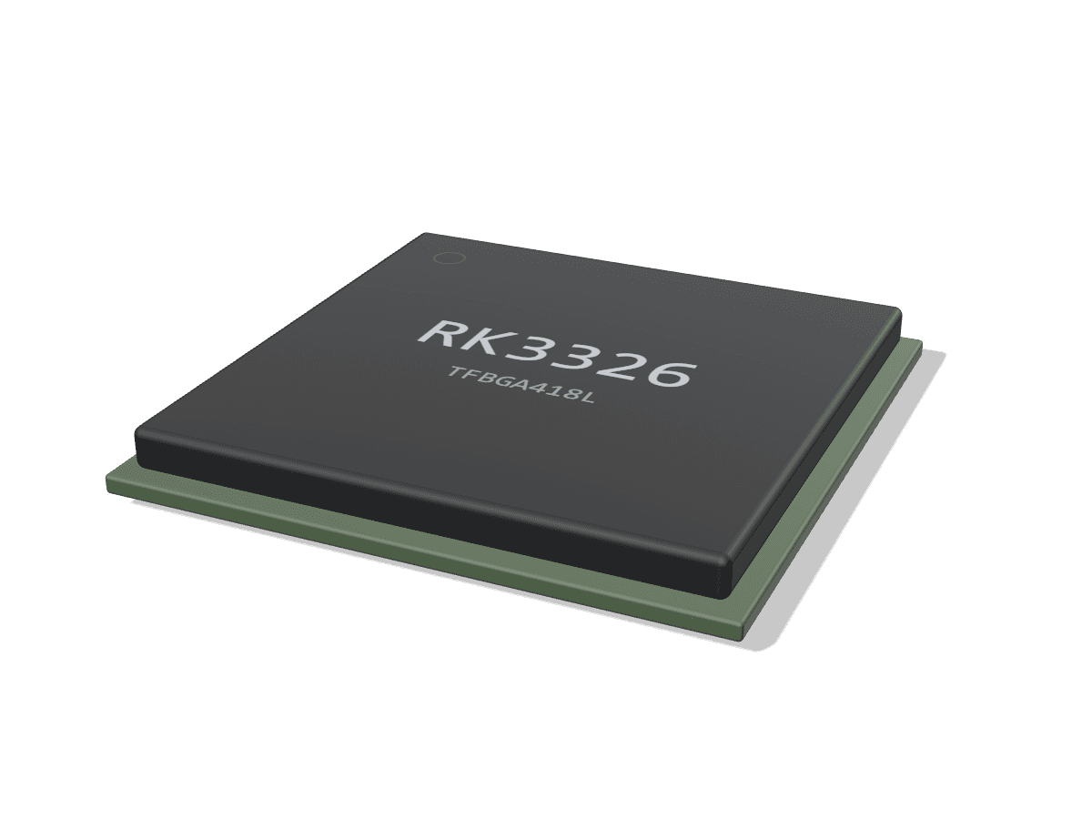
- CPU
- 4x A35, 1.3 GHz mainline, 1.5 GHz vendor
- GPU
- Mali-G31 MP2
- NPU
- None
- Video
- 1080p60 H.265/H.264 decode, 1080p H.264 encode
- PCIe
- None
What the RK3326 / PX30 is for
Right for
- Battery handhelds and portable displays: RK817 PMIC with charger and fuel gauge is the usual pairing, and mainline Linux carries ODROID-GO Advance/Super, Anbernic RG351M/V and GameForce Chi device trees
- 7 to 10 inch HMI and kiosk panels driven over MIPI DSI (4 lanes), LVDS or 24-bit RGB at up to 1920x1080
- Dual independent displays on a budget: PX30 has two display processors (VOP_BIG and VOP_LITE); RK3326 has one
- Smart audio and voice front ends: one 8-channel I2S/TDM, one 8-channel PDM microphone input and two 2-channel I2S
- Long-tail products that want mainline Linux: CPU, GPU (Panfrost), DSI, LVDS, ISP, Hantro H.264 decode and USB are upstream since 5.6 to 5.16
Wrong for
- Anything needing PCIe, SATA, USB 3 or Gigabit Ethernet: none of them exist on this die (PX30 has a single 10/100 RMII MAC, RK3326 has none)
- Edge AI: no NPU; the Mali-G31 MP2 is one double-pixel shader core
- 4K video or HDMI output: decode tops out at 1080p60, display at 1920x1080, and there is no HDMI transmitter
- Designs needing more than 4 GB DRAM or LPDDR4 on the original parts (LPDDR4 needs RK3326-S or PX30-S)
- CPU-heavy workloads: four in-order Cortex-A35 cores sharing 256 KB L2 (512 KB on RK3326-S)
Cost and constraints
- Chip cost is low: LCSC lists RK3326 at USD 8.48 and PX30 at USD 8.89 in single units, falling to about USD 6 at 100 to 119 pieces (2026-10-13)
- BOM is the SoC (TFBGA418L, 14 x 14 mm, 0.65 mm pitch), an RK817 or RK809 PMIC, one 32-bit or 16-bit DDR3/DDR3L/DDR4/LPDDR3 bank and eMMC; the Boardcon RK3326-S module is 8 layers
- Commercial parts are rated 0 to 80 C ambient; PX30K extends that to -20 to 85 C. There is no -40 C part in the family
- Mainline caps the CPU at 1.296 GHz; vendor kernels run to 1.512 GHz on PX30 and PX30-S
- RK3326-S and PX30-S are not in mainline Linux; handheld distributions carry their own patch sets for them
Inside the RK3326 / PX30
Drawn by Groundplane from the trm rev 1.1. Not Rockchip artwork.
- DDR3/3L/4, LPDDR2/3, 32-bit
- LPDDR4 on RK3326-S, PX30-S
- Up to 4 GB
- eMMC
- SD/MMC
- SPI NOR/NAND
- 8-bit NAND
- 4x Cortex-A35, Neon, FP
- 256 KB L2 (512 KB on -S)
- TrustZone, crypto extensions
- Mali-G31 MP2
- 2D engine (RGA2-Lite)
- 1080p60 H.265/H.264 decode
- 1080p H.264 encode
- JPEG encode and decode
- 8 MP ISP
- VIP parallel capture
- VOP_BIG 1920x1080
- VOP_LITE 1920x1080 (PX30)
- 32-bit DDR controller, 2 ranks
- 32 KB boot ROM, SRAM
- Crypto engine, TRNG
- Secure OTP, secure boot
- PMU, power domains
- DMAC, timers, watchdog
- TSADC, SARADC
- USB 2.0 OTG
- USB 2.0 host (PX30)
- 10/100 RMII MAC (PX30)
- SDIO 3.0
- MIPI DSI 4-lane
- LVDS
- 24-bit RGB
- MIPI CSI 4-lane
- 12-bit parallel camera
- 8-ch I2S/TDM, 8-ch PDM
- 2x 2-ch I2S
- I2C, UART, SPI, PWM
- SARADC
Read from the documents
Each value names the document it was read from.
| CPU | 4x Cortex-A35 (ARMv8-A, Neon, FP, crypto extensions), 32 KB L1 I/D each, 256 KB shared L2; max 1.5 GHz (PX30 Rev 1.6; vendor kernel OPP 1.512 GHz, mainline OPP 1.296 GHz) | Datasheet Rev 1.6, 1.2.1, Table 3-2 |
|---|---|---|
| GPU | Mali-G31 MP2 (G31-2EE): one double-pixel shader core, 64 KB L2, max 500 MHz; OpenGL ES 1.1/2.0/3.2, Vulkan 1.0, OpenCL 2.0, DirectX 11 FL9_3 | Datasheet Rev 1.6, 1.2.8, Table 3-2; TRM Part 1 ch. 4 |
| Video decode | H.265 Main up to Level 4.1, 1920x1080@60; H.264 up to High 4.1, 1080p60 (MVC Stereo High, SVC base layer); MPEG-1/2/4, VP7, VP8, H.263, RV8/9/10, JPEG, WebP | TRM Rev 1.0, ch. 4.1.1 |
| Video encode | H.264 BP/MP/HP up to level 4.1, 1920x1080@30 (or 2x 720p30); JPEG encode. H.265 decode and H.264 encode/decode share one VPU and cannot run at the same time | Datasheet Rev 1.3, 1.2.6; TRM Part 2 ch. 4.1 |
| Memory | DDR3-1600, DDR3L-1600, DDR4-1600, LPDDR2-1066, LPDDR3-1600; 32-bit (16 and 8-bit supported), 2 ranks, 4 GB total. LPDDR4 only on RK3326-S and PX30-S | Datasheet Rev 1.1, 1.2.4; TRM Part 2 ch. 2.1 |
| Storage | eMMC (8-bit), SD/MMC (4-bit), SPI NOR and SPI NAND (SFC), 8-bit async and toggle NAND; boot ROM loads from all of these | TRM Rev 1.1, ch. 1.2 |
| Display | VOP_BIG: 1920x1080 (1280x800 with CABC). VOP_LITE (PX30 only): 1920x1080. Outputs: 24-bit RGB, 4-lane MIPI DSI at 1.0 Gbps per lane to 1080p60, LVDS (RGB888/666) to 1280x800@60. RGB and DSI, or RGB and LVDS, can run at once | Datasheet Rev 1.3, 1.2.10 to 1.2.12 |
| Camera | MIPI CSI-2 RX, 4 lanes at up to 1.0 Gbps each, into the ISP (max input 3264x2448); parallel input to the VIP (8/10/12-bit raw, YCbCr422, BT.656). One MIPI and one parallel camera can run together | Datasheet Rev 1.3, 1.2.9 |
| USB | PX30: USB 2.0 OTG plus USB 2.0 host (EHCI/OHCI). RK3326: USB 2.0 OTG only | Datasheet Rev 1.3, 1.2.14; RK3326 Rev 1.4 1.2.13 |
| Ethernet | PX30: one 10/100 MAC with RMII. RK3326: none | Datasheet Rev 1.3, 1.2.14 |
| Audio | 1x 8-channel I2S/TDM, 1x 8-channel PDM, 2x 2-channel I2S/PCM, up to 192 kHz | Datasheet Rev 1.3, 1.2.13 |
| Other I/O | PX30: 4x I2C, 6x UART, 2x SPI, 8x PWM. RK3326: 3x I2C, 4x UART (Rev 1.4 corrects Rev 1.1), 2x SPI. Both: SDIO 3.0, 3-channel 10-bit SARADC, 2 temperature sensors, 4 Kbit OTP | Datasheet Rev 1.3, 1.2.14, 1.2.15; RK3326 Rev 1.4 1.2.13 |
| Security | TrustZone, crypto engine (AES, DES/TDES, SHA-1/2, MD5, HMAC, RSA/ECC to 4096-bit), TRNG, secure OTP, secure boot, DDR scrambling | Datasheet Rev 1.1, 1.2.5 |
| Package | TFBGA418L, 14 x 14 mm, 0.65 mm pitch, 0.3 mm balls (PX30, PX30K, RK3326 Rev 1.4, RK3326-S, PX30-S). RK3326 Rev 1.1 said TFBGA395L; Rev 1.4 corrects it | Datasheet Rev 1.4, 1.2.14, 2.1 |
| Power | CPU_VDD 0.95 to 1.35 V (PX30 Rev 1.6: 0.90 V min), LOGIC_VDD and PMU_VDD 0.90 to 1.10 V, I/O at 3.3 V or 1.8 V, 24 MHz crystal | Datasheet Rev 1.6, Table 3-2 |
| Temperature | PX30, RK3326, PX30-S: 0 to 80 C ambient. PX30K: -20 to 85 C. Tj max 125 C. Theta JA 26.9 C/W, theta JC 8.2 C/W (theta JB 7.2 C/W on the -S parts), 4-layer JEDEC board | Datasheet Rev 1.3, Table 3-1, 3-2, 4-1 |
Variants
| PX30 | The full part: dual display processors (VOP_BIG and VOP_LITE), 10/100 RMII Ethernet, USB 2.0 host in addition to OTG, 6 UARTs, 4 I2C, 8 PWM, 12-bit parallel camera input. Max 1.5 GHz CPU, 500 MHz GPU; 0 to 80 C ambient. | Datasheet Rev 1.6 |
|---|---|---|
| PX30K | Extended-temperature PX30 in the same TFBGA418L package: -20 to 85 C ambient against 0 to 80 C. Used on Firefly Core-PX30K-JD4 and ADLINK LEC-PX30 -R modules. | Datasheet Rev 1.3 |
| RK3326 | Consumer part on the same SoC ID: USB 2.0 OTG only, no Ethernet, one VOP, 4 UARTs and 3 I2C (Rev 1.4), 2 PWM. Same TFBGA418L package per Rev 1.4. Mainline rk3326.dtsi is px30.dtsi with VOP_LITE and its DSI and LVDS inputs deleted. | Datasheet Rev 1.4 |
| RK3326-S | Later revision: 512 KB L2 (twice the RK3326) and LPDDR4 added to DDR3/DDR3L/DDR4/LPDDR3 (32-bit, 4 GB max); 8 PWMs; theta JB 7.2 C/W published. Otherwise the RK3326 feature set in TFBGA418L. | Datasheet Rev 1.1 |
| PX30-S | Later revision of PX30: 512 KB L2 and LPDDR4 support, PX30 I/O set (Ethernet, USB host, 6 UART, 4 I2C), 0 to 80 C. Rockchip kernels detect it from an OTP field and give it its own CPU OPP table to 1.512 GHz, GPU OPP table, DRAM timing and a DMC table to 1056 MHz. | Datasheet Rev 1.1 |
What to watch when you design with it
Size a heatsink for the RK3326 / PX30 with its datasheet θJC and Tj max filled in, and download the STEP.
Power and PMIC
Two pairings show up in every board we checked. Battery products use the RK817 (bucks, LDOs, switching Li-ion charger with power path, fuel gauge and an audio codec with speaker and headphone drivers): ODROID-GO Advance/Super, Anbernic RG351M/V, GameForce Chi and Boardcon CM3326S. Mains-powered SoMs and the Rockchip EVB use the RK809 (same regulator set and codec, no charger): Firefly Core-PX30-JD4, Theobroma Ringneck and Cobra, Engicam PX30.Core. The CPU rail runs from 0.95 V at 600 MHz to 1.35 V at 1.296 GHz in the mainline OPP table. The RK817 takes 3.8 to 5.5 V USB or 2.7 to 5.5 V battery input and has four bucks (two 2.5 A, two 1.5 A), nine LDOs, a 0.08 to 3 A input-limited charger, BOOST/OTG at 2.1 A and a codec with class-D speaker driver; the RK809 adds a fifth buck (1.5 to 3.6 V, 2.5 A) and two 2.1 A switches in place of the charger, and keeps the fuel gauge and codec. Both are 7 x 7 mm QFN68.
Sources: PMIC Rev 2.1, PMIC Rev 1.8, Other V1, git.kernel.org, git.kernel.org, Other v7.3-rc7
DDR
One 32-bit controller (16 and 8-bit also supported), two ranks, 4 GB total, DDR3/DDR3L/DDR4/LPDDR2/LPDDR3 at up to 1600 (LPDDR2 1066). The -S revisions add LPDDR4: Boardcon ships 1 to 4 GB LPDDR4 on RK3326-S, and the vendor kernel gives PX30-S its own DRAM timing and a DMC table to 1056 MHz. U-Boot has an open-source PX30 DRAM init (sdram_px30.c, with DDR3, DDR4, LPDDR2 and LPDDR3 configurations); Rockchip also ships closed DDR init blobs (px30_ddr_333MHz and rk3326_ddr_333MHz, v2.12 in rkbin). No DDR layout guide exists on a host we can link; the Boardcon CM3326S is an 8-layer module.
Sources: Datasheet Rev 1.1, Datasheet Rev 1.1, TRM Rev 1.0, Other V1, Other develop-6.1, github.com, github.com
Display interfaces
The DSI and LVDS transmitters share pins with each other and with part of the RGB parallel bus: Boardcon's CM3326S pinout names its display pins LVDS/MIPI_TXDn/LCDC_Dn. Plan DSI or LVDS, not both, and check which RGB bits you lose. On PX30 each output can be fed by either VOP, which is how two different images reach two panels; RK3326 has one VOP. VOP_BIG drops to 1280x800 when content-adaptive backlight control (CABC) is enabled.
Sources: Other V1, TRM Rev 1.0, Other v7.3-rc7
Boot and maskrom
The boot ROM checks eMMC, then SPI NOR, then SPI NAND, then the SD card, and falls back to USB download on the OTG port when none holds a valid ID block, so keep the OTG port reachable. Boardcon brings out two test points beside the eMMC: shorting them at power-up forces maskrom. Its Recovery key sits on an ADC input with a 10 k pull-up, read by the loader. Rockchip's loader blobs for both parts (rk3326_ and px30_ miniloader, usbplug, BL31, BL32) are in rkbin; mainline U-Boot plus upstream TF-A also boot it.
Sources: TRM Rev 1.1, Other V2.0, Other V1, github.com
Thermal
Theta JA is 26.9 C/W and theta JC 8.2 C/W on a 4-layer JEDEC board for every part in the family; Tj max is 125 C. The PX30 datasheet notes that Rockchip reference software limits the chip to about 85 C. Commercial parts are rated 0 to 80 C ambient, PX30K -20 to 85 C. Vendor modules derate further: Firefly rates Core-PX30-JD4 at -20 to 60 C and the PX30K version at -20 to 70 C, Boardcon its RK3326-S module at 0 to 70 C.
Sources: Datasheet Rev 1.6, Datasheet Rev 1.1, Other V1.1, Other V1
Gotchas
The VPU is a combo block: H.265 decode and H.264 encode or decode cannot run at the same time. Mainline caps the CPU at 1.296 GHz although Rockchip quotes 1.5 GHz. Mainline has the Hantro decoder (H.264, VP8, MPEG-2) and JPEG encoder but not the HEVC decoder or the RGA. RK3326-S and PX30-S silicon (ROCKNIX already carries a device tree for one RK3326-S handheld) needs out-of-tree patches (TSADC, GPU power domain, DSI PHY timing, OTP, USB PHY tuning, suspend) on mainline. RK3326 datasheet Rev 1.1 (the LCSC copy, and the LCSC listings for both RK3326 and PX30) says TFBGA395L; Rev 1.4 and every PX30 revision say TFBGA418L. Lay out from the newest ball map.
Sources: TRM Rev 1.0, Other v7.3-rc7, github.com, Datasheet Rev 1.1, Datasheet Rev 1.4, Other
Layout guides for the RK3326 / PX30's interfaces
Public layout guidance for each interface this chip has, from vendors who publish it, plus our calculators.
LPDDR4
Point-to-point routing; TI notes that on-die termination on both ends means no board termination is needed. Byte lanes length-matched to their strobe and command/address matched to the clock, all over a solid reference plane. Impedance targets differ by vendor: TI AM62x and ADI EE-480 use 40 ohm single-ended and 80 ohm differential, Synaptics SL1680 uses 50 and 85 ohm, AMD Versal 45 and 82 ohm. Use the SoC vendor's own target and simulate.
- AM62x, AM62Lx DDR Board Design and Layout GuidelinesTexas Instruments, SPRAD06, C, 2025
- AM62Ax, AM62Px, AM62Dx LPDDR4 Board Design and Layout GuidelinesTexas Instruments, SPRAD66, B, 2024
- ADSP-2184x/ADSP-SC84x LPDDR4 Board Design GuidelinesAnalog Devices, EE-480, 1, 2026
- SL1680 General PCB Design and LPDDR4 & LPDDR4(x) Interface Layout GuidelinesSynaptics, PN 506-001390-01, E
- DDR length matching calculatorGroundplane calculator
DDR4
DDR4 uses pseudo open-drain data signaling and needs a VPP supply, with command/address routed fly-by or as a balanced tree depending on device count. TI AM62x uses 40 ohm single-ended and 80 ohm differential; AMD Versal uses 50 and 90 ohm, relaxed under the BGA. Match data to strobe per byte and command/address to clock.
- AM62x, AM62Lx DDR Board Design and Layout GuidelinesTexas Instruments, SPRAD06, C, 2025
- Versal Adaptive SoC PCB Design User Guide: PCB Routing Guidelines for DDR4 InterfacesAMD, UG863, 1.12, 2026
- SL1640 General PCB Design and DDR4 & LPDDR4(x) Interface Layout GuidelinesSynaptics, PN 506-001529-01, D
- PCB Design Guidelines (HSSI, EMIF, MIPI, True Differential, PDN) User Guide: Agilex 5 FPGAs and SoCsAltera, 821801, 2026
- DDR length matching calculatorGroundplane calculator
- Via current calculatorGroundplane calculator
DDR3 / DDR3L
Fly-by command/address with termination at the end of the chain, point-to-point data lanes matched to their strobe, and a clean VREF. ST recommends 55 ohm single-ended and 100 ohm differential for DDR3 and DDR3L on STM32MP1 boards, and shows that a 4-layer board is possible with strict layer allocation.
- STM32MP1 Series DDR memory routing guidelinesSTMicroelectronics, AN5122, 3, 2019
- DDR3 Design Requirements for KeyStone DevicesTexas Instruments, SPRABI1, D, 2022
- SL2610 General PCB Design and DDR3L/DDR4 & LPDDR4(x) Interface Layout GuidelinesSynaptics, PN 506-001629-01, A, 2025
- DDR length matching calculatorGroundplane calculator
LPDDR3
Point-to-point and normally unterminated, with command/address matched to the clock and each byte matched to its strobe. ST gives the same targets for LPDDR3 as for DDR3: 55 ohm single-ended and 100 ohm differential. Few current public guides cover LPDDR3, so treat the SoC vendor's reference layout as the stronger source.
- STM32MP1 Series DDR memory routing guidelinesSTMicroelectronics, AN5122, 3, 2019
- DDR length matching calculatorGroundplane calculator
eMMC
A single-ended bus: CLK, CMD, DAT0 to DAT7 and, for HS400, the data strobe. TI and Synaptics both route it at 50 ohm single-ended, match the group, and keep stubs short; Synaptics places a 22 or 33 ohm series resistor on CLK and STRB. At HS400 TI also checks the eMMC I/O supply impedance, not just the traces.
- AM62Px eMMC HS400 Board Design and Simulation GuidelinesTexas Instruments, SPRADP5, A, 2026
- Astra Machina Foundation Series eMMC ConfigurationSynaptics, PN 506-001594-01, D
- i.MX28 Layout and Design GuidelinesNXP (Freescale), AN4215, 0, 2010
SD card / SDIO
Single-ended CLK, CMD and four data lines over a solid ground plane, at constant trace width and matched length. NXP asks for clock-to-neighbor spacing greater than twice the trace height above the plane and 1.5 times for data and CMD, with 45 degree bends. UHS modes switch the I/O to 1.8 V, so a level translator often sits next to the socket.
- NVT4557/NVT4558/NVT4858 voltage-level translator layout guidelineNXP, AN13158, 1.1, 2022
- i.MX28 Layout and Design GuidelinesNXP (Freescale), AN4215, 0, 2010
- SD Physical Layer Simplified SpecificationSD Association, 9.10, 2023
USB 2.0
One D+/D- pair at 90 ohm differential, routed in parallel for its whole length with minimal deviations at the connector and package. NXP keeps clocks and periodic signals at least 50 mils away and other signals at least 20 mils away from the pair.
- High-Speed Layout Guidelines for Signal Conditioners and USB HubsTexas Instruments, SLLA414, A, 2026
- High-Speed Interface Layout GuidelinesTexas Instruments, SPRAAR7, J, 2023
- i.MX28 Layout and Design GuidelinesNXP (Freescale), AN4215, 0, 2010
MIPI DSI
MIPI D-PHY clock and data lanes are routed as 100 ohm differential pairs over a solid reference; TI Jacinto 7 allows no stubs, 2 vias per trace and 40 ps lane-to-lane skew. Connectors and flex cables to the panel are usually the largest discontinuity, so keep the board segment short and clean.
- Jacinto7 AM6x, TDA4x, and DRA8x High-Speed Interface Design GuidelinesTexas Instruments, SPRACP4, A, 2024
- PCB Design Guidelines (HSSI, EMIF, MIPI, True Differential, PDN) User Guide: Agilex 5 FPGAs and SoCsAltera, 821801, 2026
MIPI CSI-2
Same D-PHY rules as DSI: 100 ohm differential lanes in both TI guides, with lane-to-lane skew bounded (40 ps in TI Jacinto 7). Size the lane count and lane rate from the sensor's output format before routing.
- Jacinto7 AM6x, TDA4x, and DRA8x High-Speed Interface Design GuidelinesTexas Instruments, SPRACP4, A, 2024
- High-Speed Interface Layout GuidelinesTexas Instruments, SPRAAR7, J, 2023
- PCB Design Guidelines (HSSI, EMIF, MIPI, True Differential, PDN) User Guide: Agilex 5 FPGAs and SoCsAltera, 821801, 2026
- MIPI CSI-2 bandwidth calculatorGroundplane calculator
LVDS
Tightly coupled differential pairs terminated at the receiver in 100 ohm, with TI's EMI guide asking for 100 ohm differential traces within 5 percent. Keep pairs matched and away from other aggressors, and avoid stubs and reference plane gaps along the route to the panel connector.
- LVDS Owner's Manual: Including High-Speed CML and Signal ConditioningTexas Instruments, SNLA187, 4th edition, 2008
- High-Speed Layout Guidelines for Reducing EMI for LVDS SerDes DesignsTexas Instruments, SNLA302, 2018
- LVDS SerDes Gen I PCB and Interconnect Design-In GuidelinesTexas Instruments, SNLA008, A, 2018
Ethernet (RGMII / RMII)
TI routes MAC-to-PHY (MII family) traces at 50 ohm single-ended, under 6 inches, matched within 20 mils for gigabit, and the PHY-side MDI pairs at 100 ohm differential. RGMII also needs a 1.5 to 2.0 ns clock-to-data delay, added on the board or inside the MAC or PHY (RGMII-ID); decide which before layout so it is not applied twice.
- Ethernet PHY PCB Design Layout ChecklistTexas Instruments, SNLA387, 2021
- PCB Design Guideline for RGMII InterfaceRenesas, R01AN6272EJ0141, 1.41, 2026
- i.MX28 Layout and Design GuidelinesNXP (Freescale), AN4215, 0, 2010
Board-level design guides
Impedance and timing, power, thermal and ESD guidance that applies to any board around this chip.
Impedance and timing
Every high-speed interface on the board comes down to the same two numbers: the trace impedance your stackup actually gives, and the delay each trace adds. Set the stackup with your fab first, then route to its impedance table and match lengths in time, not millimeters, where the layers differ.
- High-Speed Interface Layout GuidelinesTexas Instruments, SPRAAR7, J, 2023
- PCB impedance calculatorGroundplane calculator
- PCB propagation delay calculatorGroundplane calculator
Power delivery
For each switching regulator, place and route the input capacitor first, keep the switching current loop small, and keep the switch node short. Give the SoC rails solid planes and decoupling at the balls, and size current-carrying copper and vias for the real load.
- Five steps to a great PCB layout for a step-down converterTexas Instruments, SLYT614, 2015
- AN-1149 Layout Guidelines for Switching Power SuppliesTexas Instruments, SNVA021, C, 2013
- AN-1229 SIMPLE SWITCHER PCB Layout GuidelinesTexas Instruments, SNVA054, C, 2013
- Buck converter calculatorGroundplane calculator
- LDO power dissipation calculatorGroundplane calculator
- PCB trace width calculatorGroundplane calculator
- Via current calculatorGroundplane calculator
Thermal
Theta-JA is measured on a JEDEC test board that carries most of the heat, so it does not transfer directly to a product board; use it to compare packages and use the psi metrics for estimates. Thermal vias under the package, copper area and copper thickness move the most heat into the board.
- Semiconductor and IC Package Thermal MetricsTexas Instruments, SPRA953, D, 2024
- AN-2020 Thermal Design By Insight, Not HindsightTexas Instruments, SNVA419, C, 2013
- Heatsink thermal resistance calculatorGroundplane calculator
- LDO power dissipation calculatorGroundplane calculator
ESD protection
Place the TVS as close to the connector as design rules allow, route from the connector to the TVS with no stub, and keep the protected IC further from the TVS than the TVS is from the connector. Choose parts by clamping performance and by capacitance low enough for the interface speed.
- ESD Protection Layout GuideTexas Instruments, SLVA680, A, 2022
- Reading and Understanding an ESD Protection Data SheetTexas Instruments, SLLA305, A
- TPD12S016 PCB Layout Guidelines for HDMI ESDTexas Instruments, SLLA324, 2012
- PCB conductor spacing calculator (IPC-2221)Groundplane calculator
Rockchip's hardware design guide
Rockchip's hardware design guide, EVB reference schematics and DDR templates come from Rockchip or an authorized agent, usually under NDA, or through your SoM vendor. We do not link copies circulating elsewhere. The vendor schematics and open designs on the Boards tab are real, shipped layouts on the RK3326 / PX30 and the best public reference.
BSP, mainline and toolkits
| Area | Status | Links |
|---|---|---|
| Vendor BSP kernel | Rockchip kernel trees with px30.dtsi (covering PX30, RK3326, PX30-S and RK3326-S) on develop-4.19 (4.19.232), develop-5.10 (5.10.252), develop-6.1 (6.1.172, the default branch) and develop-6.6 (6.6.89). Board vendors ship 4.19 or 5.10: Boardcon RK3326-S images use 4.19.232 for Android 12 and 5.10.160 for Debian 11.Checked 2026-10-13 | |
| Mainline Linux | px30.dtsi and the PX30 EVB from 4.20. USB 2.0 PHY and OTP 5.5. Mali-G31 GPU node, MIPI DSI with its D-PHY, LVDS and TSADC 5.6. rk3326.dtsi and ODROID-GO Advance 5.8. Engicam PX30.Core 5.11. Hantro VPU (H.264, VP8, MPEG-2 decode, JPEG encode), ISP with CSI D-PHY and SPI flash controller 5.16. I2S/TDM 6.1. ODROID-GO Super, GO Advance v1.1, Anbernic RG351M and Theobroma Ringneck 6.2. RG351V 6.8. GameForce Chi 6.10. Firefly Core-PX30-JD4 6.12. Theobroma Cobra and PP1516 6.16. VIP parallel capture 6.19. Not upstream as of 7.3-rc7: HEVC decoder, RGA, and any RK3326-S or PX30-S support.Checked 2026-10-13 | |
| GPU | Mesa Panfrost covers Mali-G31 in its Bifrost (v7) row: OpenGL ES 3.1, OpenGL 3.1, Vulkan 1.3 and OpenCL 3.0 at row level (the conformance footnote is for G52). The vendor stack uses Arm's closed Mali driver.Checked 2026-10-13 | |
| U-Boot | Mainline U-Boot supports evb-px30, Engicam PX30.Core (C.TOUCH 2.0, C.TOUCH 2.0 10.1, EDIMM 2.2), Firefly Core-PX30-JD4 (firefly-px30), Theobroma Ringneck (ringneck-px30) and ODROID-GO Advance (odroid-go2). DRAM init has an open-source driver (sdram_px30.c); BL31 comes from upstream TF-A (plat/rockchip/px30) or rkbin.Checked 2026-10-13 | |
| NPU toolkit | Not applicable: no NPU on any part in this family.Checked 2026-10-13 | |
| Video (MPP) | Rockchip MPP has entries for both rk3326 and px30: VDPU2 decoder with post-processor, VEPU2 encoder and a 1080p HEVC decoder. This is the vendor-kernel path for HEVC.Checked 2026-10-13 | |
| Android | Firefly publishes Android 8.1 firmware and SDK for Core-PX30-JD4. Boardcon ships Android 12 (kernel 4.19.232, U-Boot 2017.09) for RK3326-S.Checked 2026-10-13 | |
| Distributions | ROCKNIX builds its RK3326 image on mainline Linux 7.1.2 with its own patch set, including PX30-S support patches, and device trees for ODROID-GO Advance/Super, Anbernic RG351M/V, GameForce Chi, Powkiddy RGB10/RGB10X/RGB20S, MagicX XU10 and XU Mini M, R36S-class clones and a GKD Pixel 2 (RK3326-S). Firefly ships Ubuntu and Buildroot for Core-PX30-JD4; Boardcon ships Debian 11 and Buildroot for RK3326-S.Checked 2026-10-13 |
RK3326 / PX30 on GitHub
Repositories for this chip: vendor code, mainline work, toolkits, distributions and open hardware.
- Kernelrockchip-linux/kernelRockchip BSP kernel; RK3326 device trees are on develop-4.19 through develop-6.12, building on the px30 dtsi. Last commit 2026-08.
- Kernelhardkernel/linuxHardkernel kernel; branch odroidgoA-4.4.y is the ODROID-GO Advance kernel that the RK3326 handheld scene grew from. Last commit 2026-09.
- Kerneltorvalds/linuxMainline Linux has RK3326 device trees for the ODROID-GO Advance family on the px30 dtsi. Last commit 2026-10.
- Bootloaderrockchip-linux/rkbinDDR init and loaders; bin/rk33 holds the rk3326 binaries alongside the related px30 set. Last commit 2026-08.
- Bootloaderhardkernel/u-bootHardkernel U-Boot; branch odroidgoA-v2017.09 is the vendor bootloader for the RK3326 ODROID-GO Advance. Last commit 2026-09.
- Bootloaderu-boot/u-bootMainline U-Boot boots RK3326 through the px30 SoC code, with odroid-go2_defconfig for the ODROID-GO Advance. Last commit 2026-10.
- Mediarockchip-linux/mppMedia Process Platform; osal/mpp_soc.c includes rk3326 for its VPU. Last commit 2026-09.
- Mediaairockchip/librgaRGA 2D acceleration library with RK3326 and RK3326S in its supported chip list. Last commit 2026-06.
- DistributionROCKNIX/distributionHandheld gaming distribution whose RK3326 device ships device trees for ODROID-GO Advance, Anbernic RG351M, Powkiddy RGB10 and others. Last commit 2026-10.
- DistributionAmberELEC/AmberELECHandheld firmware for the RK3326 Anbernic RG351 series and compatible devices. Last commit 2026-10.
- Distributionchristianhaitian/arkosArkOS for RK3326 handhelds; archived in 2025 and succeeded by dArkOS. Archived. Last commit 2025-08.
- Distributionchristianhaitian/dArkOSDebian based ArkOS successor for RK3326 and RK3566 handhelds. Last commit 2026-10.
- Toolschristianhaitian/rk3326_core_buildsScripts that build RetroArch cores and emulators for RK3326 devices. Last commit 2026-10.
- Toolsrockchip-linux/rkdeveloptoolRockchip open source USB flashing tool for maskrom and loader mode, the Linux and macOS alternative to RKDevTool. Last commit 2025-03.
- Communitylcdyk0517/arkos4clonePorts ArkOS and dArkOS to unsupported RK3326 clone handhelds, with per device DTBs that document many board variants. Last commit 2026-10.
- CommunityPortsMaster/PortMaster-GUIPortMaster, the game port installer used across RK3326 handheld distributions. Last commit 2026-10.
RK3326 / PX30 system on modules
Any of these can sit on a carrier board we design.
| Module | Vendor | Connector | RAM | Design files | Price | Buy |
|---|---|---|---|---|---|---|
| Core-PX30-JD4 / Core-PX30K-JD4 | Firefly | SODIMM 260-pin gold finger, 0.5 mm pitch | 1 or 2 GB DDR3 | none (specification PDF, SDK and firmware only) | USD 169 (Firefly store, 1 GB/8 GB; one price shown across the SoM-only and carrier packages) | |
| RINGNECK SOM-PX30-uQ7 | Cherry Embedded Solutions (formerly Theobroma Systems) | micro-Qseven (MXM-230 edge) | Up to 4 GB DDR4 | none public (datasheet, user manual, source code) | ||
| PX30.Core | Engicam | EDIMM 2.0 (SODIMM-style edge) | 1 to 2 GB DDR4 | none public (hardware manual, BSP and 3D behind login) | ||
| SOM-PX30 | Geniatech | 172-pin stamp hole | 1 or 2 GB (the spec PDF gives both) | schematic PDF (25 pages, module plus reference carrier, RK809 PMIC); no layout | ||
| LEC-PX30 | ADLINK | SMARC 2.0 (short size) | 1, 2 or 4 GB DDR3L | |||
| SOM-RP301 | ARBOR | SOM-1-S | 2 GB LPDDR3 | none public (datasheet; other downloads behind login) | ||
| CM3326S | Boardcon | 156-pin castellated edge, 1.0 mm pitch | 1 to 4 GB LPDDR4 | hardware manual (pinout) and 3D model; no schematic |
Every public RK3326 / PX30 board
| Board | Vendor | Type | RAM | Notable I/O | Design files | Price | Buy |
|---|---|---|---|---|---|---|---|
| ODROID-GO Advance Black Edition | Hardkernel | Dev kit, Handheld, 155 x 72 x 20 mm; Hardkernel sells ODROID products as development platforms | 1 GB DDR3L, 32-bit | Discontinued (marked obsolete in the Hardkernel shop), 3.5 inch 320x480 MIPI DSI LCD, RK817 PMIC, 3000 mAh battery, USB 2.0 host, 10-pin I2C/GPIO header, 16 MB SPI boot flash, microSD, ESP-WROOM-S2 Wi-Fi | |||
| AIO-PX30-JD4 (MB-JD4 carrier) | Firefly | Carrier, Carrier for Core-PX30-JD4 (also takes Core-3328-JD4), 12 V DC input | RJ45 10/100 with PoE (802.3at), 4x USB 2.0 through a hub, 30-pin LVDS, MIPI CSI, mini PCIe for 3G/4G, 36-pin expansion header | none | USD 169 with Core-PX30-JD4 1 GB/8 GB (Firefly store) | ||
| C.TOUCH 2.0 | Engicam | Carrier, 115 x 72 mm, 15 to 30 V DC input | 10/100 Ethernet, Wi-Fi and BT, CAN, RS485, 2x RS232, USB-A and USB OTG, Single-channel LVDS | none public (manual and 3D behind login) | |||
| DB-PX30 | Geniatech | Carrier, 140 x 113 mm development board for SOM-PX30, 12 V input | 2 GB | RJ45 10/100, Wi-Fi and BT 4.1, USB OTG plus USB 2.0 host, 8 GB eMMC (16 or 32 GB optional) | SOM-PX30 schematic PDF only | ||
| I-Pi SMARC PX30 | ADLINK | Dev kit, I-Pi SMARC carrier with LEC-PX30 (2 GB) and a DSI-to-HDMI board | 2 GB | 2x 10/100 Ethernet, 4x USB 2.0 plus OTG, CAN | USD 89 with Wi-Fi (ipi.wiki store) | ||
| PBA-9000-A | ARBOR | Carrier, Carrier for SOM-RP301, 165 x 115 mm, 12 V input | HDMI, DSI, eDP, LVDS, Gigabit Ethernet on the carrier | ||||
| EM3326S | Boardcon | SBC, 110 x 85 mm baseboard with CM3326S, 5 V/3 A or 4.2 V Li-ion, 0 to 70 C | 1 to 4 GB LPDDR4 | 10/100 Ethernet (RTL8152B on USB), 2x USB 2.0 host plus OTG, Wi-Fi 4 and BT 4.2, mini PCIe for 4G, LVDS/MIPI DSI header, 40-pin RGB FPC, MIPI CSI, RS485 | user manual and block-level overview diagram; no schematic |
Prices and links as checked on the dates in our data; the latest check on this page was 2026-10-13.
Buying the chip
Both original parts are stocked in single units at LCSC at under USD 9, which makes prototypes easy. We found no distributor listing for PX30K, RK3326-S or PX30-S; those go through Rockchip agents or come pre-mounted on modules (Firefly and ADLINK for PX30K, Boardcon for RK3326-S). Rockchip does not publish a distributor list we could confirm.
- LCSC: RK3326 (C5182195)
- Listed as TFBGA-395L 14x14 (the Rev 1.1 package name; Rev 1.4 says TFBGA418L), full tray 1190. USD 8.48 at qty 1, 7.28 at 10, 6.56 at 30, 5.95 at 100; out of stock on 2026-10-13. MOQ 1.
- LCSC: PX30 (C2835344)
- Listed as TFBGA-395L, tray of 119 (the PX30 datasheet says TFBGA418L, 1190 per tray). USD 8.89 at qty 1, 7.57 at 10, 6.76 at 30, 6.08 at 119; 20 in stock on 2026-10-13. MOQ 1.
- Boardcon (modules)
- CM3326S RK3326-S SoM and EM3326S SBC by quote; no public pricing.
- Firefly (modules)
- Core-PX30-JD4 (1 GB/8 GB) listed at USD 169 in the Firefly store, with no separate SoM-only price shown; 198 in stock on 2026-10-13. A PX30K version is specified.
Datasheet, TRM and design documents
Linked where they are publicly hosted; we do not rehost Rockchip documents. These are third-party documents: we are not responsible for their accuracy, availability or confidentiality status. Disclosure.
- DatasheetRockchip RK3326 DatasheetRev 1.1 · 2018-04-11 · hosted by LCSC · checked 2026-10-13
- DatasheetRockchip RK3326 Datasheet (newest; corrects package to TFBGA418L)Rev 1.4 · 2019-01-10 · community mirror (rockchip.fr), not hosted by Rockchip · checked 2026-10-13
- DatasheetRockchip PX30 / PX30K DatasheetRev 1.3 · 2019-04-28 · hosted by Macro Group · checked 2026-10-13
- DatasheetRockchip PX30 / PX30K Datasheet (newest; adds max CPU and GPU clock)Rev 1.6 · 2021-07-06 · community mirror (rockchip.fr), not hosted by Rockchip · checked 2026-10-13
- DatasheetRockchip RK3326-S DatasheetRev 1.1 · 2022-03-01 · community mirror (rockchip.fr), not hosted by Rockchip · checked 2026-10-13
- DatasheetRockchip PX30-S DatasheetRev 1.1 · 2022-04-12 · community mirror (rockchip.fr), not hosted by Rockchip · checked 2026-10-13
- TRMRockchip PX30 TRM Part 1 (also covers RK3326)Rev 1.1 · 2018-09-17 · community mirror (rockchip.fr), not hosted by Rockchip · checked 2026-10-13
- TRMRockchip PX30 TRM Part 2 (also covers RK3326)Rev 1.0 · 2018-08-13 · community mirror (rockchip.fr), not hosted by Rockchip · checked 2026-10-13
- PMICRockchip RK817 Datasheet (battery PMIC with charger and codec)Rev 2.1 · 2023-03-20 · hosted by LCSC · checked 2026-10-13
- PMICRockchip RK809 Datasheet (PMIC with codec, no charger)Rev 1.8 · 2021-10-29 · hosted by LCSC · checked 2026-10-13
- Product briefRockchip RK3326 product pagehosted by Rockchip · checked 2026-10-13
- Product briefRockchip PX30 product pagehosted by Rockchip · checked 2026-10-13
- OtherLCSC part listing: Rockchip RK3326 (C5182195)hosted by LCSC · checked 2026-10-13
- OtherLCSC part listing: Rockchip PX30 (C2835344)hosted by LCSC · checked 2026-10-13
- OtherFirefly Core-PX30-JD4 / Core-PX30K-JD4 specificationV1.1 · 2023-12-26 · hosted by Firefly · checked 2026-10-13
- OtherCherry RINGNECK SOM-PX30-uQ7 datasheet1.3 · 2024-04-22 · hosted by Cherry Embedded Solutions · checked 2026-10-13
- OtherBoardcon CM3326S (RK3326-S SoM) hardware manualV1 · 2023-03-26 · hosted by Boardcon · checked 2026-10-13
- OtherBoardcon EM3326S (RK3326-S SBC) user manualV2.0 · 2023-12-25 · hosted by Boardcon · checked 2026-10-13
- OtherRockchip vendor kernel px30.dtsi (PX30, RK3326, PX30-S, RK3326-S)develop-6.1 · hosted by Rockchip (GitHub) · checked 2026-10-13
- OtherMainline Linux px30.dtsiv7.3-rc7 · hosted by kernel.org · checked 2026-10-13
- OtherMainline Linux rk3326.dtsiv7.3-rc7 · hosted by kernel.org · checked 2026-10-13
Questions about the RK3326 / PX30
Not the RK3326 / PX30 itself. We have designed and brought up boards on the Rockchip RV1106, RV1126, RV1126B, RK3566, RK3568, RK3576 and RK3588, and on the Allwinner T507 and A527/T527. The work carries over: power tree, DDR and high-speed layout, bring-up and the BSP, read against this chip's own datasheet.
They share one SoC ID, one TRM and the same TFBGA418L package. PX30 adds a second display processor (two independent displays), a 10/100 RMII Ethernet MAC, a USB 2.0 host port, more UARTs, I2C and PWM, and a 12-bit parallel camera input; RK3326 has USB 2.0 OTG only. Mainline Linux builds rk3326.dtsi by deleting the second VOP from px30.dtsi. CPU, GPU, video and memory blocks are the same.
LCSC hosts RK3326 Rev 1.1 (April 2018) and Macro Group hosts PX30 Rev 1.3 (April 2019). Newer revisions (RK3326 Rev 1.4, PX30 Rev 1.6) and the RK3326-S and PX30-S datasheets are only on the rockchip.fr mirror, as is the PX30 TRM (Part 1 Rev 1.1, Part 2 Rev 1.0), which also covers the RK3326. Use RK3326 Rev 1.4 for layout: it corrects the package from TFBGA395L to TFBGA418L.
Later revisions of the same chips with 512 KB L2 (instead of 256 KB) and LPDDR4 support, in the same TFBGA418L package. Rockchip kernels give PX30-S its own CPU, GPU and DRAM operating points and detect it from OTP. Mainline Linux does not support either yet, and handheld distributions such as ROCKNIX carry patches for them.
Yes, for the original parts. CPU, Mali-G31 (Panfrost), MIPI DSI, LVDS, USB 2.0, ISP and the Hantro H.264/VP8/MPEG-2 decoder are upstream by 5.16, and boards from Hardkernel, Anbernic, GameForce, Engicam, Firefly and Theobroma have upstream device trees. The HEVC decoder and RGA are not upstream, and mainline limits the CPU to 1.296 GHz against the 1.5 GHz datasheet maximum.
No. For on-device inference in this price class look at RK3566 or RV1106; the RK3326 only has its Mali-G31 MP2 GPU and four Cortex-A35 cores.
Firefly Core-PX30-JD4 (260-pin SODIMM, USD 169 in its store), ADLINK LEC-PX30 (SMARC 2.0, also as the USD 89 I-Pi SMARC kit), Cherry RINGNECK (micro-Qseven), Engicam PX30.Core (EDIMM 2.0), Geniatech SOM-PX30 (172-pin stamp hole) and ARBOR SOM-RP301. For RK3326-S there is Boardcon CM3326S. Only Geniatech publishes a schematic; none publishes layout.
Related chips and reading
- RK3566HMI, e-ink readers, handhelds, CM4-class SoMs, small routers
- RK3308Smart speakers, mic arrays, audio bridges, gateways
- RK3328Routers, TV boxes, Klipper hosts
- RK3128 / RK3126TV boxes, tablets, low-cost HMIs
- RV1106 / RV1103Small AI cameras, tiny Linux nodes, IP KVMs
- RK3562Cost-down HMI, tablets, industrial gateways
We'll design your RK3326 board.
Tell us the interfaces, power budget and volume. An engineer replies with questions or a proposal.
Links and facts on this page checked 2026-10-13. Spotted something out of date? Tell us through the contact form.
Compiled from publicly available sources: datasheets, technical reference manuals, vendor product pages, schematics and source code published by their owners and third parties. We link to documents where others host them and do not host, endorse or vouch for them. Everything on these pages, including our own specs, summaries, block diagrams, comparisons, calculators and design notes, is for reference only and may contain errors or be out of date. It is provided as is, and Groundplane is not responsible for errors in it, for third-party documents, or for any design, board or decision based on it. Always check the manufacturer's current datasheet, reference manual and design guidance before you design a board. Rockchip, Allwinner, Raspberry Pi and other product names are trademarks of their owners; we are not affiliated with any of them. See our disclosure.