V853 / V851
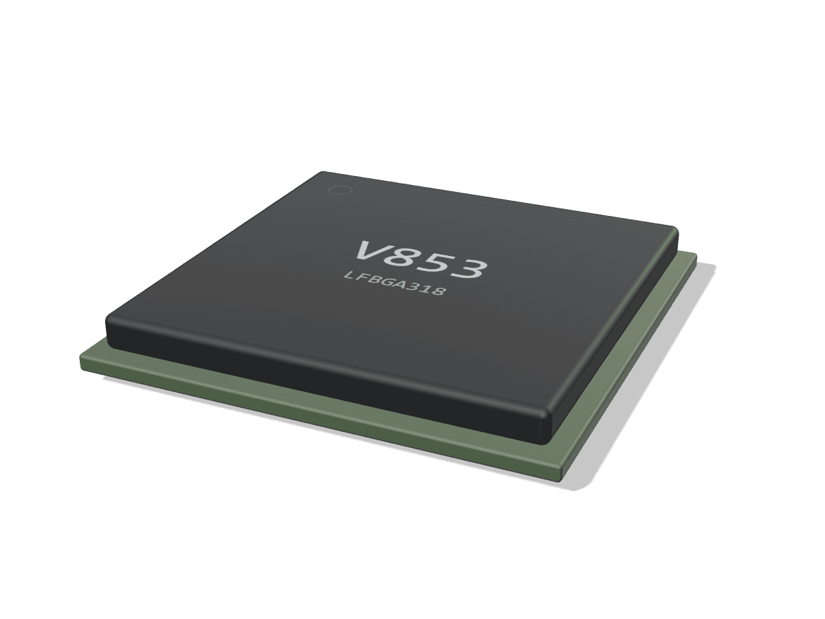
Allwinner's AI camera family: one Cortex-A7 plus a RISC-V E907 core, a 0.5 to 1 TOPS NPU and a 5MP ISP. The V853 takes external 16-bit DDR3/DDR3L up to 1 GB on an LFBGA318; the V851S/SE put 64 MB DDR2 in a QFN88 at the cost of 4MP capture and 10/100 Ethernet. Software is Allwinner's Tina Linux on a 4.9 kernel.
- CPU
- 1x A7 + RISC-V E907
- GPU
- None (G2D only)
- NPU
- 0.5 to 1 TOPS
- Video
- Enc 5M@25 H.265/H.264, dec H.264
- PCIe
- None
What the V853 / V851 is for
Right for
- Smart cameras that need on-device detection: a 1 TOPS NPU (V853) or 0.5 TOPS (V851S/SE) beside a 5MP@30 (V853) or 4MP@30 (V851S) ISP and an H.265/H.264 encoder
- Displays on a camera product: the V853 drives 4-lane MIPI DSI up to 1920x1200@60 or parallel RGB up to 1920x1080@60, which the RV1106 cannot
- Lowest-cost Linux camera boards with no DDR routing: the V851S/SE QFN88 carries 64 MB DDR2 inside the package, and the V851SE adds a 10/100 Ethernet PHY
- Designs that want a separate real-time core: the RISC-V E907 at 600 MHz runs an RTOS alongside Linux on the Cortex-A7 (Allwinner ships E907 firmware examples for its V853 board)
- Gigabit wired cameras: the V853 EMAC supports 10/100/1000 over RGMII
Wrong for
- Anything that needs mainline Linux today: as of Linux 7.3-rc7 only a V853 pinctrl binding (6.14) and the PPU power-domain driver (6.15) are upstream, with no SoC devicetree or clock driver
- General compute or desktop Linux: one Cortex-A7 at 1 GHz (900 MHz on the V851S) and no 3D GPU
- HDMI output, PCIe, SATA or USB 3: none exist; USB is a single USB 2.0 dual-role port
- More than 1 GB of RAM: the DRAM controller is 16-bit DDR3/DDR3L with a 1 GB ceiling, and the V853S and V851 parts are fixed at 128 MB or 64 MB in package
- Projects that cannot work through Chinese-language channels: the SDK download needs an Allwinner Online account and most community support is in Chinese
Cost and constraints
- LCSC single-unit pricing on 2026-10-13: V853 USD 5.94 (USD 3.70 at 1008), V851S USD 15.46, so the BGA V853 is the cheaper chip at LCSC but needs external DDR3 and a BGA-capable board
- Memory is part of the part number on the V853S (128 MB DDR3L) and V851S/V851SE (64 MB DDR2); only the V853 has an external DRAM bus
- The V851SE trades the display interfaces and SPI1 for an in-package 10/100 PHY: it has no MIPI DSI and no parallel LCD
- Vendor software is Tina Linux on kernel 4.9 and U-Boot 2018; newer kernels exist only as community ports
- The V853 datasheet defers all PCB guidance to a V853/V853S hardware design guide that is not public, and states no power consumption figures (it says to contact an Allwinner FAE)
Inside the V853 / V851
Drawn by Groundplane from the product brief v1.4. Not Allwinner artwork.
- DDR3/DDR3L 16-bit (V853 only)
- eMMC 5.1 / SD 3.0
- SPI NOR / SPI NAND
- 1x Cortex-A7 up to 1 GHz, FPU
- 32 KB + 32 KB L1, 128 KB L2
- RISC-V E907 at 600 MHz
- 1 TOPS (V853), 0.8 (V853S)
- 0.5 TOPS (V851S/SE)
- 128 KB internal buffer
- H.265 / H.264 encode, 5M@25
- H.264 / JPEG decode
- JPEG encode, 1080p@60
- G2D: rotate, mix, scale
- ISP 5M@30 (V851: 4M@30)
- Four VIPP outputs
- WDR, 2D/3D NR, 3A
- 16-bit DDR3/DDR3L to 1 GB
- V853S: 128 MB DDR3L in package
- V851S/SE: 64 MB DDR2 in package
- Display engine: 2 video + 1 UI
- TCON LCD and MIPI DSI
- Crypto: AES, 3DES, RSA, ECC, SHA
- TRNG, 2 Kbit OTP
- TrustZone, secure boot
- CCU, GIC, DMA, IOMMU
- Thermal sensor, timers
- Audio codec: 1 DAC, 2 ADC
- USB 2.0 dual-role
- GbE MAC, RGMII/RMII (V853)
- SDIO 3.0 for Wi-Fi
- MIPI CSI 1x 4-lane or 2x 2-lane
- Parallel CSI to 16-bit
- MIPI DSI 4-lane, RGB LCD
- 5x TWI, 4x UART, 4x SPI
- 12x PWM, 4x GPADC
- I2S x2, DMIC, Wiegand in
Read from the documents
Each value names the document it was read from.
| CPU | 1x Cortex-A7 at up to 1 GHz with FPU, 32 KB I + 32 KB D L1, 128 KB L2; plus a RISC-V core at 600 MHz with 16 KB I + 16 KB D cache | Product brief V1.4, Features: CPU |
|---|---|---|
| CPU clock (V851S/SE) | Cortex-A7 at 900 MHz, RISC-V at 600 MHz | Datasheet Rev 0.1, 1.1 |
| NPU | V853 up to 1 TOPS, V853S 0.8 TOPS; INT8/INT16 hybrid; 128 KB internal buffer; frameworks TensorFlow, Caffe, TFLite, PyTorch, ONNX | Datasheet Rev 1.1, 1.1, Table 1-1, 1.3.3 |
| NPU (V851S/SE) | Up to 0.5 TOPS, 128 KB internal buffer | Datasheet Rev 0.1, 1.3.3 |
| GPU | No 3D GPU. Display engine with 2 video channels and 1 UI channel; G2D 2D accelerator (rotate, mixer, scaler) | Product brief V1.4, Features: Display Engine |
| Video encode | H.264 BP/MP/HP and H.265 MP, up to 4K@15 or 5M@25 (brief); multi-stream 5M@25; JPEG to 1080p@60 | Product brief V1.4, Features: Video Engine |
| Video encode (V851S/SE) | H.264/H.265 encoder rated 3840x2160@20 at 400 MHz, multi-stream 5M@25 + 720p@25; up to 8 ROIs; CBR, VBR, FIXQP; JPEG 1080p@60 | Datasheet Rev 0.1, 1.3.4 |
| Video decode | H.264 (BP/MP/HP) and JPEG; 5M@25 H.264 in the block diagram | Product brief V1.4, Features: Video Engine; Block Diagram |
| Video decode (V851S/SE) | H.264 and JPEG decoding, maximum decode resolution 4096x4096 | Datasheet Rev 0.1, 1.3.4 |
| ISP | V853: 5M@30, max 3072x1772; adjustable AE, AWB, AF; four VIPP YUV422/420 outputs to 5M@30 | Product brief V1.4, Features: Video Input |
| ISP (V851S/SE) | One ISP, 2560x1440 online, 4M@30; offline mode; 2-frame WDR, DRC, 2D/3D NR, DPC, CAC; four VIPPs with crop and 1 to 1/16 scaling | Datasheet Rev 0.1, 1.3.6.1, 1.3.6.2 |
| Camera | V853: one 4-lane MIPI CSI (splittable to two 2-lane, DOL WDR, 4-channel VC de-interleave) to 5M@30; 8/10/12/16-bit parallel CSI (BT.601, BT.656, BT.1120) to 5M@30; up to 4-ch AHD or 3-ch RAW interleaved input | Product brief V1.4, Highlight; Features: Video Input |
| Camera (V851S/SE) | One 4-lane or two 2-lane MIPI CSI, CSI-2 v1.00, D-PHY v1.00, 1.2 Gbps per lane, to 4M@30; 10-bit parallel CSI (BT.601/656), 148.5 MHz pixel clock | Datasheet Rev 0.1, 1.3.6.3, 1.3.6.4 |
| Memory | V853: one 16-bit channel of DDR3/DDR3L (1.5 V or 1.35 V), 2 chip selects, up to 933 MHz, up to 1 GB; controller runs in half-rate mode. V853S: 128 MB DDR3L in package | Datasheet Rev 1.1, 4.1, Table 1-1 |
| Memory (V851S/SE) | 64 MB DDR2 in package (SIP); no external DRAM interface | Datasheet Rev 0.1, 1.1, Table 1-1 |
| Storage | SD 3.0 / eMMC 5.1 (V851S/SE: eMMC 4.5), SPI NOR and SPI NAND; three SD/MMC host controllers (SMHC x3) | Product brief V1.4, Features: Memory; Block Diagram |
| Display | V853: 4-lane MIPI DSI up to 1920x1200@60; RGB LCD up to 1920x1080@60 | Product brief V1.4, Features: Video OUT |
| Display (V851S) | 2-lane MIPI DSI (v1.02, D-PHY v1.2, 1.0 Gbps per lane) up to 1280x720@60; TCON LCD with i8080 and serial RGB to 800x480@60, parallel RGB DE/SYNC, BT.656. The V851SE has no MIPI DSI and no LCD | Datasheet Rev 0.1, 1.3.5 |
| PCIe | None | Product brief V1.4 |
| USB | 1x USB 2.0 DRD (host or device) | Product brief V1.4, Features: Connectivity |
| Ethernet | V853: 1x 10/100/1000 EMAC, RMII or RGMII to an external PHY, full and half duplex, jumbo frames to 16 KB, 2 KB TX and 8 KB RX FIFO | Datasheet Rev 1.1, 9.1 |
| Ethernet (V851S/SE) | V851S: 10/100 EMAC with RMII. V851SE: 10/100 Ethernet PHY in package, no external EMAC pins | Datasheet Rev 0.1, Table 1-1 |
| Audio | Codec with 1 DAC and 2 ADCs: MICIN1P/N, MICIN2P/N, LINEOUTP/N; 2x I2S/PCM; DMIC | Product brief V1.4, Features: Audio |
| Audio (V851S/SE) | Codec with 1 DAC (8 to 192 kHz) and 1 ADC (8 to 48 kHz), one differential mic input, single-ended line out; 1x I2S/PCM (I2S1) up to 16 channels; DMIC up to 8 PDM mics | Datasheet Rev 0.1, 1.3.7 |
| Security | Crypto engine (AES, DES, 3DES; RSA/ECC; MD5, SHA, HMAC), PRNG and TRNG, 2 Kbit OTP, TrustZone, secure boot, security ID | Product brief V1.4, Features: Security System; Block Diagram |
| Other I/O | 5x TWI, 4x UART, 4x SPI (SPI NAND/NOR capable), 12-channel PWM, 4-channel GPADC, SDIO 3.0, Wiegand input | Product brief V1.4, Features: Connectivity |
| Other I/O (V851S/SE) | 5x TWI, 4x UART, 4x SPI (3 on the V851SE), 11-channel PWM, 1-channel GPADC, Wiegand input | Datasheet Rev 0.1, 1.3.8 |
| Process | 22 nm | Product brief V1.4, Overview |
| Package | V853: LFBGA318, 12 x 12 mm, 0.5 mm ball pitch | Product brief V1.4, Features: Package |
| Package handling | V853/V853S: MSL3; 168 per tray, 1680 per inner box, 10080 per carton. Pin count V853: 199 I/O, 24 power, 81 GND, 5 DDR power, 9 NC | Datasheet Rev 1.1, Table 2-1, 12.1, 12.2.1 |
| Package (V851S/SE) | QFN88, 9 x 9 mm, 0.35 mm pitch | Datasheet Rev 0.1, 2.1.1 |
| Temperature | V853/V853S: ambient -20 to 70 C, junction -40 to 115 C | Datasheet Rev 1.1, Table 2-6 |
| Temperature (V851S/SE) | Ambient -20 to 70 C, junction -40 to 115 C | Datasheet Rev 0.1, Table 2-6 |
| Thermal | V853 theta-JA 32.45, theta-JB 10.85, theta-JC 10.83 C/W; V853S 29.12, 11.08, 11.15 C/W (JEDEC 2S2P, still air, simulated) | Datasheet Rev 1.1, Tables 2-4, 2-5 |
| Thermal (V851S) | Theta-JA 21.1, theta-JB 6.5, theta-JC 4.15 C/W (JEDEC 2S2P, still air, simulated) | Datasheet Rev 0.1, Table 2-4 |
| Power domains | V853: VDD-SYS 0.9 V (0.81 to 1.0), VDD09-USB 0.9 V, VCC-DRAM 1.5 V DDR3 or 1.35 V DDR3L, VDD18-DRAM 1.8 V, AVCC, VCC-PLL, VCC-RTC and MIPI rails 1.8 V, VCC-IO, VDD33 and VCC33-USB 3.3 V; ports PA, PC, PD, PE, PG, PI selectable 1.8 or 3.3 V | Datasheet Rev 1.1, Table 2-6 |
| Boot | Boot ROM boots SD/eMMC, SPI NOR and SPI NAND; medium chosen by two GPIO pins or eFuse; mandatory upgrade (FEL) over USB or SMHC0; normal and secure boot | Datasheet Rev 1.1, 3.5 |
Variants
| V853 | 1 TOPS NPU, external 16-bit DDR3/DDR3L up to 1 GB, 5M@30 ISP, 4-lane MIPI DSI to 1920x1200, gigabit EMAC (RGMII), LFBGA318 12 x 12 mm. | Product brief V1.4 |
|---|---|---|
| V853S | NPU rated 0.8 TOPS instead of 1 TOPS, and 128 MB DDR3L in the package in place of the external DRAM bus, in the same LFBGA318 (fewer I/O balls: 145 against 199). Slightly lower theta-JA (29.12 against 32.45 C/W). | Datasheet Rev 1.1 |
| V851S | 900 MHz Cortex-A7, 0.5 TOPS NPU, 64 MB DDR2 in package, 4M@30 ISP and capture (2560x1440), 2-lane MIPI DSI to 1280x720 plus parallel/serial RGB and i8080 LCD, 10/100 EMAC (RMII), 4x SPI, QFN88 9 x 9 mm. | Datasheet Rev 0.1 |
| V851SE | The V851S with a 10/100 Ethernet PHY in the package and no external EMAC pins; no MIPI DSI and no LCD interface; 3 SPI instead of 4; GPIO in 5 ports (PA, PC, PE, PF, PH) instead of 6. | Datasheet Rev 0.1 |
What to watch when you design with it
Power and PMIC
Allwinner's own V853 development board uses the AXP2101 PMIC (which Allwinner describes as its own design; the datasheet is copyright Shenzhen X-Powers), which accepts DC 12 V, USB 5 V or a single Li-ion cell and talks to the SoC over TWI; Allwinner notes it is a general-purpose PMU with unused outputs switched off. The AXP2101 gives 5 bucks (DCDC1 1.5 to 3.4 V at 2 A; DCDC2 and DCDC3 down to 0.5 V at 2 A; DCDC4 1.5 A; DCDC5 1 A) and 11 LDOs in a 5 x 5 mm QFN-40. For the V851S/SE the datasheet shows only three externally supplied rails in its power-on example: 3.3 V I/O, 1.5 V DDR2 and 0.9 V VDD-SYS, with 1.8 V analog rails made by the internal LDOA, so small boards build the tree from discrete regulators.
Sources: PMIC V1.0, Board schematic, Datasheet Rev 0.1
Power sequencing (V851S/SE)
Per the V851S datasheet: VCC33-PF and PD ramp first; VDD-SYS must ramp at least 1 ms after LDOA and VCC-PLL are stable and at least 8 ms before reset is released; the 24 MHz clock starts 4 ms after reset release. At power-off all rails ramp down together. VDD-SYS is 0.81 to 1.0 V (0.9 V typical) and VCC-DRAM 1.425 to 1.575 V for the in-package DDR2.
Sources: Datasheet Rev 0.1
Power sequencing (V853/V853S)
Per the V853 datasheet: VCC-RTC must ramp no later than any other rail; reset starts to ramp at least 8 ms after VDD-SYS is stable; the 24 MHz clock starts 4 ms after reset is released. In the example sequence the 1.8 V and 3.3 V I/O rails follow the DRAM and core rails within 0 to 4 ms. At power-off all rails ramp down together. Absolute maximums: 1.08 V on VDD-SYS, 2.16 V on the 1.8 V rails, 3.96 V on the 3.3 V rails.
Sources: Datasheet Rev 1.1
DDR
Only the V853 has an external DRAM bus: one 16-bit channel of DDR3 or DDR3L, up to 1 GB, rated to 933 MHz with 2 chip selects and 1.5 V or 1.35 V I/O. The datasheet gives DDR3 command and address timing at 800 MHz (tIS 170 ps and tIH 120 ps minimum). Allwinner's board uses a single Rayson RS256M16 DDR3 (512 MB, BGA96). Its hardware notes say the DQ lines may be swapped within each byte lane (SDQ0 to 7 with DQS0 and DQM0; SDQ8 to 15 with DQS1 and DQM1) to ease routing, and that the controller supports two DRAM devices or one dual-rank device. The public design rules stop there; the V853/V853S hardware design guide that the datasheet points to for PCB recommendations is not public. The V853S, V851S and V851SE have their DRAM in the package, so there is nothing to route but the capacity is fixed by part number.
Sources: Datasheet Rev 1.1, Product brief V1.4, Board schematic
Boot and FEL
The boot ROM reads two boot-select pins (Allwinner's board uses PC2 and PC3 with pull-ups or pull-downs) or eFuse. On the V853 board the four settings give the orders: SPI NAND, SPI NOR, USB FEL; SPI NOR first (fast boot), then SPI NAND, USB FEL; SD0, SPI NAND, SPI NOR, UART burn, USB FEL; and the default SD0, SPI NOR, eMMC user, eMMC boot, SPI NAND, UART burn, USB FEL. A dedicated FEL pin forces USB download mode: on Allwinner's board it is the UBOOT key, on the Lizard a FEL button. The open-source xfel tool has a V851/V853 chip driver for FEL download and flashing.
Sources: Datasheet Rev 1.1, Board schematic, github.com, linux-sunxi.org
Camera and display
The V853's single 4-lane CSI port splits into two 2-lane ports, which is how Allwinner's board runs two GC2063 1080p sensors from one 40-pin FPC; the parallel CSI shares pins with the RMII Ethernet and Bluetooth on that board (port PE), so check the mux before assigning both. The same board brings out both MIPI DSI (shared with RGB on port PD) and an RGB666 connector. On the V851S the CSI is 1.2 Gbps per lane and ISP input tops out at 2560x1440, so 5MP sensors need the V853.
Sources: Board schematic, Datasheet Rev 0.1
Thermal
Allwinner gives simulated values on a JEDEC 2S2P board in still air. V853 LFBGA318: theta-JA 32.45, theta-JB 10.85, theta-JC 10.83 C/W; V853S: 29.12, 11.08, 11.15 C/W. V851S QFN88: 21.1, 6.5, 4.15 C/W. All parts are rated -20 to 70 C ambient with junction at or below 115 C. The datasheets publish no power consumption figures, so size the thermal path from measurements on your own board.
Sources: Datasheet Rev 1.1, Datasheet Rev 0.1
Gotchas
Brief and datasheet disagree on encode: the V853 brief says 4K@15 or 5M@25, the V853 and V851S datasheets say 3840x2160@20 at 400 MHz. The brief rates the DRAM to 933 MHz while the datasheet timing table is given at 800 MHz. The V851SE has no display output at all. The SDK repository on sdk.aw-ol.com requires an Allwinner Online login. Allwinner's V853 board uses a 100 Mbit PHY (IP101GR) over RMII even though the V853 MAC supports gigabit RGMII.
Sources: Product brief V1.4, Datasheet Rev 1.1, Datasheet Rev 0.1, docs.aw-ol.com, Board schematic
Layout guides for the V853 / V851's interfaces
Public layout guidance for each interface this chip has, from vendors who publish it, plus our calculators.
DDR3 / DDR3L
Fly-by command/address with termination at the end of the chain, point-to-point data lanes matched to their strobe, and a clean VREF. ST recommends 55 ohm single-ended and 100 ohm differential for DDR3 and DDR3L on STM32MP1 boards, and shows that a 4-layer board is possible with strict layer allocation.
- STM32MP1 Series DDR memory routing guidelinesSTMicroelectronics, AN5122, 3, 2019
- DDR3 Design Requirements for KeyStone DevicesTexas Instruments, SPRABI1, D, 2022
- SL2610 General PCB Design and DDR3L/DDR4 & LPDDR4(x) Interface Layout GuidelinesSynaptics, PN 506-001629-01, A, 2025
- DDR length matching calculatorGroundplane calculator
eMMC
A single-ended bus: CLK, CMD, DAT0 to DAT7 and, for HS400, the data strobe. TI and Synaptics both route it at 50 ohm single-ended, match the group, and keep stubs short; Synaptics places a 22 or 33 ohm series resistor on CLK and STRB. At HS400 TI also checks the eMMC I/O supply impedance, not just the traces.
- AM62Px eMMC HS400 Board Design and Simulation GuidelinesTexas Instruments, SPRADP5, A, 2026
- Astra Machina Foundation Series eMMC ConfigurationSynaptics, PN 506-001594-01, D
- i.MX28 Layout and Design GuidelinesNXP (Freescale), AN4215, 0, 2010
SD card / SDIO
Single-ended CLK, CMD and four data lines over a solid ground plane, at constant trace width and matched length. NXP asks for clock-to-neighbor spacing greater than twice the trace height above the plane and 1.5 times for data and CMD, with 45 degree bends. UHS modes switch the I/O to 1.8 V, so a level translator often sits next to the socket.
- NVT4557/NVT4558/NVT4858 voltage-level translator layout guidelineNXP, AN13158, 1.1, 2022
- i.MX28 Layout and Design GuidelinesNXP (Freescale), AN4215, 0, 2010
- SD Physical Layer Simplified SpecificationSD Association, 9.10, 2023
PCIe
AC-coupled differential lanes routed with no stubs, minimal vias and back-drilled or blind vias where speed demands, with lane-to-lane skew handled by the receiver. Targets differ by guide: TI Jacinto 7 uses 85 ohm differential for lanes and 100 ohm for the reference clock, while TI's earlier SoC guide tabulates 100 ohm and, for some devices, 95 ohm. Match the target to your connector and stackup.
- Jacinto7 AM6x, TDA4x, and DRA8x High-Speed Interface Design GuidelinesTexas Instruments, SPRACP4, A, 2024
- High-Speed Interface Layout GuidelinesTexas Instruments, SPRAAR7, J, 2023
USB 3.x
SuperSpeed TX and RX pairs are routed at 90 ohm differential in all three TI guides (SPRAAR7 lists 95 ohm for some devices), with AC coupling capacitors on TX, symmetric pad and via placement, and matched via counts within each pair. Keep the pairs away from the USB 2.0 pair and other aggressors, and place ESD at the connector.
- High-Speed Layout Guidelines for Signal Conditioners and USB HubsTexas Instruments, SLLA414, A, 2026
- Jacinto7 AM6x, TDA4x, and DRA8x High-Speed Interface Design GuidelinesTexas Instruments, SPRACP4, A, 2024
- High-Speed Interface Layout GuidelinesTexas Instruments, SPRAAR7, J, 2023
USB 2.0
One D+/D- pair at 90 ohm differential, routed in parallel for its whole length with minimal deviations at the connector and package. NXP keeps clocks and periodic signals at least 50 mils away and other signals at least 20 mils away from the pair.
- High-Speed Layout Guidelines for Signal Conditioners and USB HubsTexas Instruments, SLLA414, A, 2026
- High-Speed Interface Layout GuidelinesTexas Instruments, SPRAAR7, J, 2023
- i.MX28 Layout and Design GuidelinesNXP (Freescale), AN4215, 0, 2010
MIPI DSI
MIPI D-PHY clock and data lanes are routed as 100 ohm differential pairs over a solid reference; TI Jacinto 7 allows no stubs, 2 vias per trace and 40 ps lane-to-lane skew. Connectors and flex cables to the panel are usually the largest discontinuity, so keep the board segment short and clean.
- Jacinto7 AM6x, TDA4x, and DRA8x High-Speed Interface Design GuidelinesTexas Instruments, SPRACP4, A, 2024
- PCB Design Guidelines (HSSI, EMIF, MIPI, True Differential, PDN) User Guide: Agilex 5 FPGAs and SoCsAltera, 821801, 2026
MIPI CSI-2
Same D-PHY rules as DSI: 100 ohm differential lanes in both TI guides, with lane-to-lane skew bounded (40 ps in TI Jacinto 7). Size the lane count and lane rate from the sensor's output format before routing.
- Jacinto7 AM6x, TDA4x, and DRA8x High-Speed Interface Design GuidelinesTexas Instruments, SPRACP4, A, 2024
- High-Speed Interface Layout GuidelinesTexas Instruments, SPRAAR7, J, 2023
- PCB Design Guidelines (HSSI, EMIF, MIPI, True Differential, PDN) User Guide: Agilex 5 FPGAs and SoCsAltera, 821801, 2026
- MIPI CSI-2 bandwidth calculatorGroundplane calculator
Ethernet (RGMII / RMII)
TI routes MAC-to-PHY (MII family) traces at 50 ohm single-ended, under 6 inches, matched within 20 mils for gigabit, and the PHY-side MDI pairs at 100 ohm differential. RGMII also needs a 1.5 to 2.0 ns clock-to-data delay, added on the board or inside the MAC or PHY (RGMII-ID); decide which before layout so it is not applied twice.
- Ethernet PHY PCB Design Layout ChecklistTexas Instruments, SNLA387, 2021
- PCB Design Guideline for RGMII InterfaceRenesas, R01AN6272EJ0141, 1.41, 2026
- i.MX28 Layout and Design GuidelinesNXP (Freescale), AN4215, 0, 2010
Board-level design guides
Impedance and timing, power, thermal and ESD guidance that applies to any board around this chip.
Impedance and timing
Every high-speed interface on the board comes down to the same two numbers: the trace impedance your stackup actually gives, and the delay each trace adds. Set the stackup with your fab first, then route to its impedance table and match lengths in time, not millimeters, where the layers differ.
- High-Speed Interface Layout GuidelinesTexas Instruments, SPRAAR7, J, 2023
- PCB impedance calculatorGroundplane calculator
- PCB propagation delay calculatorGroundplane calculator
Power delivery
For each switching regulator, place and route the input capacitor first, keep the switching current loop small, and keep the switch node short. Give the SoC rails solid planes and decoupling at the balls, and size current-carrying copper and vias for the real load.
- Five steps to a great PCB layout for a step-down converterTexas Instruments, SLYT614, 2015
- AN-1149 Layout Guidelines for Switching Power SuppliesTexas Instruments, SNVA021, C, 2013
- AN-1229 SIMPLE SWITCHER PCB Layout GuidelinesTexas Instruments, SNVA054, C, 2013
- Buck converter calculatorGroundplane calculator
- LDO power dissipation calculatorGroundplane calculator
- PCB trace width calculatorGroundplane calculator
- Via current calculatorGroundplane calculator
Thermal
Theta-JA is measured on a JEDEC test board that carries most of the heat, so it does not transfer directly to a product board; use it to compare packages and use the psi metrics for estimates. Thermal vias under the package, copper area and copper thickness move the most heat into the board.
- Semiconductor and IC Package Thermal MetricsTexas Instruments, SPRA953, D, 2024
- AN-2020 Thermal Design By Insight, Not HindsightTexas Instruments, SNVA419, C, 2013
- Heatsink thermal resistance calculatorGroundplane calculator
- LDO power dissipation calculatorGroundplane calculator
ESD protection
Place the TVS as close to the connector as design rules allow, route from the connector to the TVS with no stub, and keep the protected IC further from the TVS than the TVS is from the connector. Choose parts by clamping performance and by capacitance low enough for the interface speed.
- ESD Protection Layout GuideTexas Instruments, SLVA680, A, 2022
- Reading and Understanding an ESD Protection Data SheetTexas Instruments, SLLA305, A
- TPD12S016 PCB Layout Guidelines for HDMI ESDTexas Instruments, SLLA324, 2012
- PCB conductor spacing calculator (IPC-2221)Groundplane calculator
Allwinner's hardware design guide
Allwinner's hardware design guide, EVB reference schematics and DDR templates come from Allwinner or an authorized agent, usually under NDA, or through your SoM vendor. We do not link copies circulating elsewhere. The vendor schematics and open designs on the Boards tab are real, shipped layouts on the V853 / V851 and the best public reference.
BSP, mainline and toolkits
| Area | Status | Links |
|---|---|---|
| Vendor BSP kernel | Tina Linux (Allwinner's OpenWrt-derived SDK, Tina 5.0 for the V853) on Linux 4.9 and U-Boot 2018, per Allwinner's V853 board documentation. The SDK is fetched with repo from sdk.aw-ol.com and needs an Allwinner Online account. Tina 5.0 supports OpenWrt and Buildroot builds. 100ASK and DongshanPI republish board-specific Tina SDKs on GitHub.Checked 2026-10-13 | |
| Mainline Linux | Partial groundwork only. Linux 6.14 added the allwinner,sun8i-v853-pinctrl devicetree binding and Linux 6.15 added V853 support to the sun20i PPU power-domain driver (both by Andras Szemzo). As of 7.3-rc7 (2026-10-12) there is no V853 or V851 SoC devicetree, no clock (CCU) driver and no V853 entry in the sunxi pinctrl drivers. linux-sunxi notes that most V851S peripherals match blocks already supported for the D1 and that the chip has two CCUs. A community tree exists: 916BGAI/linux-v853.Checked 2026-10-13 | |
| U-Boot | No V853 or V851 support in mainline U-Boot v2026.10 (arch/arm/mach-sunxi has no such target). Vendor U-Boot 2018 in Tina. Open alternatives: awboot (supports the V851s) and xboot; xfel handles FEL download, DRAM init and SPI flashing.Checked 2026-10-13 | |
| NPU toolkit | Allwinner's NPU flow converts models with the Acuity toolkit into NBG files and runs them through the VIPLite API; the Tina NPU guide lists INT8, UINT8 and INT16 quantization and Caffe, TensorFlow, ONNX, TFLite, Keras, Darknet and PyTorch import. linux-sunxi describes the NPU as appearing to be Vivante IP. 100ASK publishes YOLOv3, YOLOv5 and other deployment walkthroughs for the V853.Checked 2026-10-13 | |
| RISC-V core | The E907 runs its own firmware alongside Linux; Allwinner publishes E907 test firmware with rpmsg and rpbuf for its V853 board.Checked 2026-10-13 | |
| Distributions | Tina OpenWrt and Buildroot images from Allwinner Online and board vendors. OpenIPC carries a v851s_lite firmware config. A Yocto layer for the Lizard (meta-yuzukilizard-v851s) exists.Checked 2026-10-13 | |
| Community | Allwinner Online (bbs.aw-ol.com) is the official developer forum and hosts the briefs, the V851S datasheet and board files; 100ASK runs V853 and V851s forum categories. All are mainly Chinese-language. linux-sunxi has V853, V851s and Lizard pages.Checked 2026-10-13 |
Every public V853 / V851 board
| Board | Vendor | Type | RAM | Notable I/O | Design files | Buy |
|---|---|---|---|---|---|---|
| V853 Development Board | Allwinner Online (designed by Sochip) | Dev kit, 118 x 75 mm, 4-layer | 512 MB DDR3 | 8 GB eMMC, XR829 Wi-Fi / BT, 10/100 Ethernet (IP101GR), MIPI DSI + RGB LCD, 7 inch panel, Dual GC2063 camera module, AXP2101 PMIC | schematic PDF, schematic source (.DSN), BOM, assembly drawing and a "design files by Sochip" pack on Allwinner Online downloads (login required) | |
| 100ASK V853-Pro | 100ASK (DongshanPI) | Dev kit, Core board plus full-function carrier | Two display interfaces (RGB, MIPI DSI), Two camera interfaces, Four USB Type-A, Onboard Wi-Fi and Bluetooth | none found in the vendor documentation | ||
| Yuzukilizard (Youmu Pi Lizard) | YuzukiHD, produced by 100ASK | Dev kit | 64 MB DDR2 in package (V851S) | 128 MB SPI NAND, TF slot, XR829 Wi-Fi / BT, 2-lane MIPI DSI, 2-lane MIPI CSI, USB-UART bridge | schematic PDF, Gerbers, BOM and placement, EasyEDA Pro and Altium projects (CERN-OHL-S-2.0) |
Prices and links as checked on the dates in our data; the latest check on this page was 2026-10-13.
Boards with published design files
| Project | Author | Files | Tool | License |
|---|---|---|---|---|
| Yuzukilizard (V851S) | YuzukiHD (repository mirrored by SoCXin) | schematic PDF, placement PDF, Gerbers and stencil, BOM and coordinates, EasyEDA Pro project, Altium project | EasyEDA | CERN-OHL-S-2.0 |
Buying the chip
Allwinner does not publish a distributor list we could confirm. LCSC stocks the V853 and V851S with public pricing; no stock listing was confirmed for the V853S or V851SE.
- LCSC: V853 (C5137799)
- USD 5.94 at 1, 4.56 at 30, 4.05 at 168, 3.70 at 1008; 81 in stock; LFBGA-318.
- LCSC: V851s (C5365286)
- USD 15.46 at 1, falling to 12.05 at 100; 204 in stock; QFN-88.
Datasheet, TRM and design documents
Linked where they are publicly hosted; we do not rehost Allwinner documents. These are third-party documents: we are not responsible for their accuracy, availability or confidentiality status. Disclosure.
- DatasheetV853&V853S DatasheetRev 1.1 · 2022-03-23 · hosted by Allwinner Online · checked 2026-10-13
- Product briefV853 Brief (High-Performance AI Vision Processor)V1.4 · hosted by Allwinner Online · checked 2026-10-13
- Product briefV853 Brief (LCSC copy, C5137799)V1.4 · hosted by LCSC · checked 2026-10-13
- DatasheetV851S&V851SE Datasheet (draft)Rev 0.1 · 2022-04-20 · hosted by Allwinner Online · checked 2026-10-13
- Product briefV851S Brief (Intelligent Professional IP Camera SoC, draft)V0.1 · hosted by Allwinner Online · checked 2026-10-13
- Product briefV851S Brief (LCSC copy, C5365286)V0.1 · hosted by LCSC · checked 2026-10-13
- PMICAXP2101 Datasheet (single-cell NVDC PMU)V1.0 · 2021-05-31 · hosted by Allwinner Online · checked 2026-10-13
- Board schematicV853 development board schematic walkthrough (Chinese)hosted by Allwinner Online docs · checked 2026-10-13
- Board schematicV853 document downloads: dev board schematic (2022-06-24), DSN, BOM, briefs (login required to download)hosted by Allwinner Online · checked 2026-10-13
- Otherlinux-sunxi V853 chip page (features, V853S NPU rating)hosted by linux-sunxi · checked 2026-10-13
- OtherPSA Certified Level 1 listing: V853, V853s, V851S, V851SE (certificate 0716053550552-10010, issued 2022-08-26)hosted by PSA Certified · checked 2026-10-13
Questions about the V853 / V851
Not the V853 / V851 itself. We have designed and brought up boards on the Allwinner T507 and A527/T527, and on the Rockchip RV1106, RV1126, RV1126B, RK3566, RK3568, RK3576 and RK3588. The work carries over: power tree, DDR and high-speed layout, bring-up and the BSP, read against this chip's own datasheet.
The newest public copy is the V853&V853S Datasheet Rev 1.1 (2022-03-23), hosted by Allwinner Online, Allwinner's developer site. It runs to about 1175 pages and includes the register descriptions, so it doubles as the user manual. The V853 Brief V1.4 is on Allwinner Online and LCSC, and the V851S&V851SE Datasheet Rev 0.1 draft (2022-04-20) is on Allwinner Online. The V853 hardware design guide it refers to for PCB rules is not public.
V853: 1 TOPS NPU, external 16-bit DDR3/DDR3L to 1 GB, 5MP ISP, 4-lane DSI, gigabit MAC, LFBGA318. V853S: same package, 128 MB DDR3L inside and 0.8 TOPS. V851S: QFN88 with 64 MB DDR2 inside, 900 MHz, 0.5 TOPS, 4MP ISP, 2-lane DSI, 10/100 RMII MAC. V851SE: the V851S with an internal 10/100 PHY but no display output. A later V851S3 with 128 MB DDR3L is reported, but no linkable Allwinner document for it was found.
All three are Cortex-A7 camera SoCs with an NPU (one core on the V853 and RV1106, four on the RV1126). The V853 sits between them: 1 TOPS like the RV1106, but with external DDR3 up to 1 GB, a gigabit MAC, an H.264 decoder and 4-lane MIPI DSI, which the RV1106 lacks; the RV1126 has four A7 cores, 2 TOPS and 4K encode. The V851S/SE is the closer RV1106 counterpart: QFN with DRAM in package and 10/100 Ethernet. Rockchip has the stronger English documentation and SDK access.
No. As of Linux 7.3-rc7 only a V853 pinctrl devicetree binding (6.14) and a PPU power-domain entry (6.15) are upstream; there is no SoC devicetree or clock driver. Products use Tina Linux on kernel 4.9. Community ports exist (for example 916BGAI/linux-v853).
Convert the model with Allwinner's Acuity toolkit to an NBG file, then run it through the VIPLite API in Tina Linux. Quantization is INT8, UINT8 or INT16. 100ASK publishes YOLOv3, YOLOv5 and LeNet walkthroughs for the V853-Pro.
Yes. The Yuzukilizard (V851S) is published with schematic, layout projects and Gerbers under CERN-OHL-S-2.0. YuzukiHD's Project Yosemite (V853) and TinyVision (V851SE) also publish their files, but they are not linked here because their repositories also rehost material we never link (an AXP2101 design guide and a DRAM template in Yosemite, Allwinner's V851 QFN88 reference design in TinyVision). Allwinner Online posts its V853 board schematic, DSN source and BOM, behind a login.
Related chips and reading
- RV1106 / RV1103Small AI cameras, tiny Linux nodes, IP KVMs
- RV1126 / RV1109AI IP cameras, access control
- RV1126BAI IP cameras, multi-camera vision
- T113HMI panels, CAN gateways, car displays, small Linux controllers
- D1 / D1sRISC-V Linux learning boards, HMI panels, digital frames, small display and audio products
We'll design your V853 board.
Tell us the interfaces, power budget and volume. An engineer replies with questions or a proposal.
Links and facts on this page checked 2026-10-13. Spotted something out of date? Tell us through the contact form.
Compiled from publicly available sources: datasheets, technical reference manuals, vendor product pages, schematics and source code published by their owners and third parties. We link to documents where others host them and do not host, endorse or vouch for them. Everything on these pages, including our own specs, summaries, block diagrams, comparisons, calculators and design notes, is for reference only and may contain errors or be out of date. It is provided as is, and Groundplane is not responsible for errors in it, for third-party documents, or for any design, board or decision based on it. Always check the manufacturer's current datasheet, reference manual and design guidance before you design a board. Rockchip, Allwinner, Raspberry Pi and other product names are trademarks of their owners; we are not affiliated with any of them. See our disclosure.